Lab 02: Number Systems and Waveforms
Objective
- Learn various number systems, including binary, decimal, octal, and hexadecimal.
- Understand the functioning of binary and MOD-N counters.
- Learn to connect and interpret signals using an oscilloscope.
Required Reading Materials
- Textbook: Digital Design: with an introduction to the Verilog HDL, 5th edition, Mano and Ciletti, ISBN-13: 978-0-13-277420-8
1-1 through 1-4, and 6-3 - Datasheet: 7493 Decade and Binary Counters
Components Required
| Component/Device | Description | Quantity |
|---|---|---|
| 7493 Ripple Counter | × 1 |
Experiments
Every experiment section that requires you to build a circuit and test it has an asterisk (*). For those sections:
- For the in-class lab: Demonstrate the working circuit to your lab instructor.
- For online lab: Take a video to describe your circuit, upload the video to YouTube, and put the link in the report.
Exp #2.1 Number Systems
Here is a quick review of number systems:
- Humans use the decimal number system, which is base 10 because we have 10 fingers.
- Digital logic systems, such as computers and microcontrollers, use binary which is base 2 because they are built using transistors. We saw in Experiment 1 that a transistor is an electrical switch that is on or off and thus has two states. A binary digit is known as a "bit" and 8 bits are called a "byte".
- Hexadecimal (base 16) and Octal (base 8) are shorthand for binary. Both are powers of two; i.e. 16 = 24 and 8 = 23. Digits in a binary number (bits) can be grouped together to convert to either hexadecimal or octal. Groupings must start at the least significant bit of the number. To convert to hexadecimal, group by 4 bits and convert each grouping into the corresponding hex digit (where 10 through 15 are represented using letters A through F). To convert to octal, group by 3 bits and convert each grouping into the corresponding octal digit.
Binary (Base 2) Number Example:
${(1010\;0101)_2} = (1) \times {2^7} + (0) \times {2^6} + (1) \times {2^5} + (0) \times {2^4} + (0) \times {2^3} + (1) \times {2^2} + (0) \times {2^1} + (1) \times {2^0}$
Binary to Decimal (Base 10) Conversion Example:
${(1010\;0101)_2} = {\left( {\matrix{{128} & {64} & {32} & {16} & 8 & 4 & 2 & 1 \cr 1 & 0 & 1 & 0 & 0 & 1 & 0 & 1 \cr} } \right)_2} \to 128 + 32 + 4 + 1 = {165_{10}} = (1) \times {10^2} + (6) \times {10^1} + (5) \times {10^0}$
Binary to Hexadecimal (Base 16) Conversion Example: (A=10, B=11, C=12, D=13, E=14, F=15)
${(1010\;0101)_2} = {\left( {\underline {\matrix{8 & 4 & 2 & 1 \cr 1 & 0 & 1 & 0 \cr} } \quad \underline {\matrix{8 & 4 & 2 & 1 \cr 0 & 1 & 0 & 1 \cr} } } \right)_2} \to A{5_{16}} = (10) \times {16^1} + (5) \times {16^0}$
Binary to Octal (Base 8) Conversion Example:
${(1010\;0101)_2} = {\left( {\underline {\matrix{4 & 2 & 1 \cr 0 & 1 & 0 \cr} } \quad \underline {\matrix{4 & 2 & 1 \cr 1 & 0 & 0 \cr} } \quad \underline {\matrix{4 & 2 & 1 \cr 1 & 0 & 1 \cr} } } \right)_2} \to {245_8} = (2) \times {8^2} + (4) \times {8^1} + (5) \times {8^0}$
Complete the math in the above examples to verify that (1010 0101)2, 16510, A516, and 2458 are the same number, just represented in a different base.
Question
- Which base, hex or octal, is more commonly used today as a shorthand representation for binary numbers and why?
To answer, refer to Table 2.1 and consider the following:- Which base, hex or octal, will require fewer digits to represent a binary number? And
- Given that a byte is comprised of 8 bits, which base, hex or octal, can be more compactly used to represent an 8-bit (1-byte) binary number?
Table 2.1: Numbers 0 to 31 and 56 to 71 in decimal (base 10), binary (base 2), octal (base 8), and hexadecimal (base 16).
Exp #2.2 * Modulo-16 Counter Using 7493
Refer to Figure 2.1 below. The 7493 chip is a 4-bit "modulo-16" counter. "Modulo N" implies that the highest digit is N-1. In this case, N-1 = 15, so the 7493 counts from 0 to 15 (F in hex) and returns to 0 on the 16th count. The counter outputs QD, QC, QB, and QA are displayed on the LEDs, and the RO(1) reset pin (pin 2) is grounded to allow the 7493 to count.
(Note, that RO(1) and RO(2) reset inputs are connected internally such that if both of them are high, the counter is forced into a reset condition with count frozen at 0000. So it's necessary to ground either or both reset inputs (pins 2 and 3) to enable counting to proceed.)
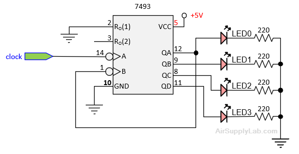
Figure 2.1: Circuit Diagram for a Mod-16 Counter
Figure 2.2 illustrates how to place the 7493 chip on the board. It should straddle at the centerline of the breadboard section. The five holes along each vertical row are connected together below the breadboard surface. A chip's pin will occupy one of the holes, so you can connect up to four wires to the same pin on that row (or connect two wires together if there is not a pin from a chip at that row).
Notice the wiring in this circuit. Where possible, the wires lay flat close to the board and do not cross one another. Avoid putting wires over the chip, as it will be difficult to remove a bad chip without having to rewire the circuit. Taking the time to wire circuits neatly will save you a lot of time in troubleshooting your circuits (finding mistakes, also known as "bugs").
![]()
Figure 2.2: 7493 Circuit Connection on the Breadboard
Question
- Draw the wire connections for the Circuit Diagram below:
- Connect the clock pin (pin 14 on the 7493 chip) to the manually controlled clock source P1 (connector 14 on the breadboard as shown in Figure 2.4.1 below)
- You can copy-paste Figure 2.3 to a PowerPoint slide and draw the connections in the PowerPoint. Copy the final connections you draw in PowerPoint to your report.
- Or, you can print out Figure 2.3 and then hand-draw it on the paper. Take a picture of your hand drawing and paste it on your report.
Exp #2.2.1 Circuit Connection for On-Campus Lab
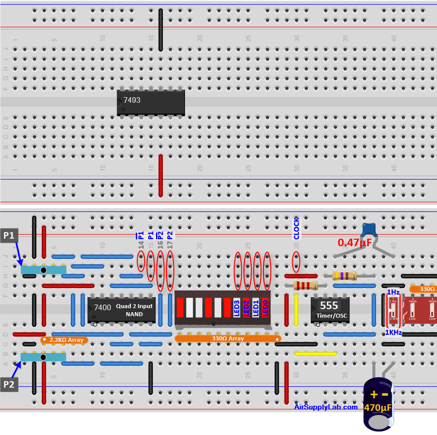
Figure 2.3: Draw the Wire Connections for Figure 2.1 Circuit on this diagram
After you draw the connections in Figure 2.3, wire up the circuit on your breadboard. As you make the connections, it is a good idea to put a checkmark on your diagram next to each wire you added so you know what part of the circuit you have completed and to ensure you do not forget any wires.
Now, connect a clock source to the circuit.
Exp #2.2.2 Circuit Connection for On-Campus Lab
Connect to a Manually Controlled Clock Source
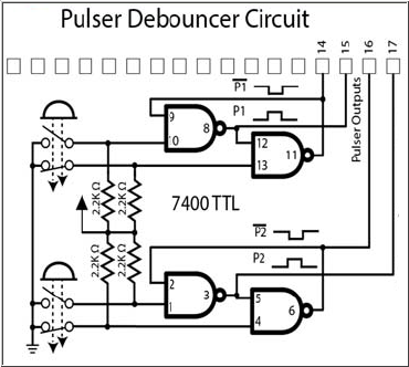
Figure 2.4.1: Pulser Debouncer Circuit
For clock signal, do not connect directly to a push-button — its output needs first to be "denounced". So it is the denounced output you will connect to. In the following diagram, there are two pulsers (push-buttons) on the left side. If you use the upper one, its "debounced" output is available in rows 14 or 15; if you use the lower one, its denounced output is in rows 16 or 17. The debouncing is done by the four NAND gates to produce a clean pulse. Refer to KB07 to learn why debouncing is needed and how it works.
The Figure on the right shows the 7493 Circuit with a clock input connected to the normally-high pulser output, and the counter's four outputs connected to the LED bargraph. The count showing on the LED bargraph is 10112 (i.e., 1110 or B16)
Pulse the clock repeatedly and verify that the counter cycles through the count 0000 to 1111. (Depending on the state of the counter when the chip powers up, the starting value will likely not be 0000, but eventually, it will count up to 1111 and then roll over to 0000 so you can observe a complete count cycle.)
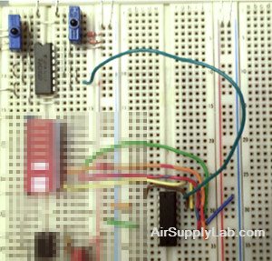
Figure 2.4.2: Connecting to a Manually Controlled Clock Source
Connect to 1 Hz Clock Source from 555 Timer
Now, connect the timer output to the counter's clock input at pin 14 (as shown in Figure 2.3). Run the clock at its slowest rate so you can see the LEDs flash on and off. (For the slowest rate, the capacitor select switch--lower left--should be flipped opposite to the way it is shown.) Again, the LEDs should go through a full 16-count sequence: 0000 → 0001 → 0010 → … → 1110 → 1111 → 0000 → .... etc.
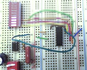
Figure 2.4.3: Counter Circuit with Clock Input Connected to 555 Timer (Row 30 on the Breadboard)
Note: if you haven't wired a circuit before, the photos in Figures 2.4.2 and 2.4.3 are provided to help. But, while you are connecting the wires to the chip, try as well to follow the wiring diagram in Figure 2.2 since for the rest of the experiments, you will only be given or will design your own wiring diagrams.
Question
- Once you finish the experiment, take a picture of your circuit connection on the breadboard and paste it on the report.
Exp #2.3 * Oscilloscope/Logic Analyzer
Once you are satisfied that the counter is running correctly, change the frequency of the square waveform to 1 KHz. The counter outputs should now be changing too fast to see their bit patterns on the LEDs, which should appear to be on all the time. Instead, you will observe counter outputs using an oscilloscope or a logic analyzer.
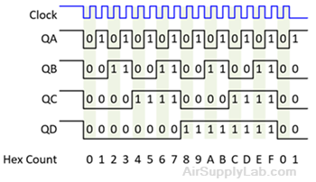
Figure 2.5: Expected Waveforms for a Mod-16 Counter
Figure 2.5 shows the timing relationships between the counter outputs. The count values are shown at the bottom of the figure; each one represents the binary pattern in the corresponding vertical slice read from the bottom up; i.e. from QD up to QA. For example, count 7 corresponds to QD, QC, QB, QA = 0 1 1 1.
Exp #2.3 Circuit Connection for On-Campus Lab
In this section, you will display the waveforms of Figure 2.5 two at a time on an oscilloscope.
- Bring QD to channel 1 and QC to channel 2.
- Set vertical sensitivity (Volts/Div) for QD and QC to 2 V/Div. Each waveform should swing approximately between 0 and 4 volts.
- Set up the scope to trigger on the negative edge (or slope) of channel 1 (i.e., QD).
- Adjust the scope-trace speed (Time/Div) so you see QD and QC displayed as in Figure 2.5 (i.e., a full cycle of QD and two full cycles of QC).
- Position the display with the Horizontal control so the point where QD goes low is on a vertical grid line near the left side of the screen, as shown below.
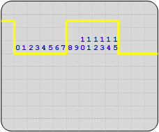
- Adjust Vertical position control for QD and QC so their 0V indicators lie on horizontal grid lines.
Important: To make it easy to read the binary count at any point in the display, do the following:
- Adjust the scope's Time/Div setting until 16 counts — the time for one cycle of QD — take up 8 divisions on the screen.
- Each division will represent 2 counts. Thus QA will toggle each half-division, QB each division, QC each two-division, and QD each four.
Verify the timing relationship between QD and QC is as in Figure 2.5.
Repeat with QD and QB on the screen, then with QD and QA, and finally with QD and the clock. Do not change any scope setting while doing this — QD should appear the same each time. Show each display to your instructor (once you have verified that it works properly, you should be able to demonstrate it to the instructor quickly by moving the wire connected to channel 2 from QC to QB to QA).
Question
- Take screenshots of the following connections from the oscilloscope:
- Connect AIN (channel 1) to QD, and BIN (channel 2) to QC.
- Connect AIN (channel 1) to QD, and BIN (channel 2) to QB.
- Connect AIN (channel 1) to QD, and BIN (channel 2) to QA.
- Connect AIN (channel 1) to QD, and BIN (channel 2) to the clock source (pin 14 on 7493).
Exp #2.4 * Mod-N Counter
As discussed in the previous sections, the counter you are using is a "modulo-16" (mod-16 or hexadecimal) counter since it counts from 0 to 15 (F in hex) and returns naturally to 0 on the 16th count. In general, a counter that counts up to a maximum value of N-1 and resets to 0 on the Nth count, can be called a modulo-N (or "mod-N") counter. Now, consider converting a 4-bit mod-16 counter into a mod-N counter with N < 16. Such a counter needs to reset to 0 on a count lower than 16, but it will not do that unless it is forced to reset prematurely. For example, a mod-14 counter (N = 14) should count up to a maximum of only 13 and then reset to 0 on the 14th count. The counter's reset inputs, RO(1), and RO(2) can be used to force this to happen.
With the asynchronous 7493, the counter must enter state N for just a few nanoseconds in order to be cleared. (As we'll see in later experiments, with a synchronous counter, the count never enters state N, but goes directly from state N-1 to 0000.) In state N, certain Q outputs will be 1's. You can combine these in such a way that they make both reset inputs RO(1) and RO(2) go high and thereby trigger an immediate reset just after state N is entered.
For example, setting up a decimal counter with N=5, observe that the binary equivalent of decimal 5 is (0101)2, where bit 0 and bit 1 are set to high. Upon reaching this state, if both pin 2 and pin 3 of the TTL7493 Counter are high, the counter's internal logic is designed to reset the count to 0000. Therefore, establish a connection from QC (bit 2) to RO(1) (Pin2) and from QA (bit 0) to RO(2) (Pin 3). As the counter progresses, it bypasses the visual transition into state 5 due to an almost instantaneous reset. Consequently, it will appear as though the counter is incrementing from 0 to 4, completing five states, before it resets to 0 and recommences the count.
Design a mod-N counter. Your instructor should give you a value for N from the set {5, 6, 8, 9, 10, 12}. If not, you can select the N value based on your group number:
$N = \left\{ \matrix{
9\quad \; \Rightarrow Group \# = \{ 1, 4, 7 \} \hfill \cr
10\quad \Rightarrow Group \# = \{ 2, 5, 8 \} \hfill \cr
12\quad \Rightarrow Group \# = \{ 3, 6 \} \hfill \cr} \right.$
As you connect your circuit, be sure to remove any grounding wires you connected to RO(1) (Pin2) and RO(2) (Pin3) as shown in Figure 2.7. If you don't, your circuit will never reset to 0 when the count reaches N. Instead, it will continue past N and reset as usual on the 16th count.
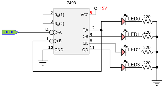
Figure 2.7: Mod-N Counter Circuit (You have to complete the drawing)
Question
- In your lab report, draw the Circuit Diagram (wiring in Figure 2.7) for your Mod-N counter circuit.
Test your design with a 1 Hz clock source or a pulser and observe the count on the LED. It should count from 0 to (N-1) in decimal numbers; otherwise, you have to check the reset circuits in your design.
Next, bring the counter outputs to the scope as in Exp #2.3. Use a 1 KHz clock source and again trigger on the falling edge of QD.
Question
- This time, record QD-QC, QD-QB, and QD-QA from the scope display and paste them into your report.
- Connect AIN (channel 1) to QD, and BIN (channel 2) to QC.
- Connect AIN (channel 1) to QD, and BIN (channel 2) to QB.
- Connect AIN (channel 1) to QD, and BIN (channel 2) to QA.
The diagram shown in Figure 2.8 is for N = 13. The display starts at the left shortly before QD goes low to trigger a new cycle of 13. The count proceeds from 0000 to 1100 (12) for a total of 13 full count periods. It then enters 1101 (13) just long enough to reset itself to 0000 again. In binary, the sequence 12-13-0 looks like 1100 > 1101 > 0000. Notice that QA (bit 0) goes to 1 as the count reaches 13. You can see this in Figure 2.8 below at the end of count 12. QA shows a short spike as it brings the count to 13. It rises and then immediately falls, having reset all the Q's, including itself, to 0. This spike is much too narrow to be seen with the scope settings you will be using since it only lasts about 50 nanoseconds. But it is there (it must be, or what else would reset the counter?).
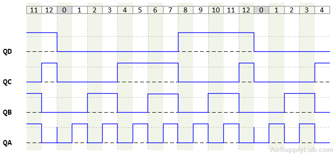
Figure 2.8: Expected Waveforms for a Mod-13 Counter.
Question
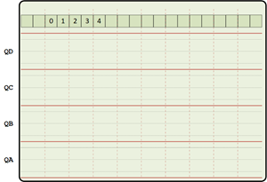
- After you have designed and tested your Mod-N counter, you have to draw the waveforms you observed on the oscilloscope to the figure below. As done in Figures 2.5 and 2.8, stack the waveforms for QA, QB, QC, and QD (even though you can only observe two at a time). You can click on the following Figure, right-click to save the image file to your local disk, then draw the signals on the image file and copy it into your report.
- For example, in a counter set to N = 13, the counting sequence progresses from 12 (1100)2 to 13 (1101)2, and then instantly resets to 0 (0000)2. This sequence demonstrates bit 0 switching from 0 to 1 and then back to 0 rapidly, resulting in a noticeable spike in the QA signal during the shift from 12 back to 0. This explains the presence of the spike in QA observed in the transition from 12 to 0, as illustrated in Figure 2.8. For your value of N, take the same approach to show which Q should spike during the reset sequence.
Exp #2.5 The 7493 Ripple Counter (Optional Reading)
The 7493 consists of 4 flip-flops with J-K inputs unconnected. In a TTL chip, unconnected inputs behave as logic 1, so J=K=1. As a result, each flip-flop is configured as a "T" and will toggle every time it is clocked; i.e. when its clock voltage falls (the 7493 has a negative edge-triggered clock input). Refer to the diagrams of the 7493 on the EE2449-Lab KB03: TTL IC Specifications.
QB, QC, QD are chained together to form a 3-bit counter; the output of each is connected internally to the clock of the next (QB goes to QC's clock, etc.). For a 4-bit counter, QA must likewise go to QB's clock but there is no such connection inside the chip. Therefore, the connection must be made externally (pin 12 to pin 1). In the resulting counter, QD is the most significant bit (MSb); i.e. the 4-bit counter output is [QD QC QB QA]. Clock pulses are input at pin 14.
The reset inputs RO(1) and RO(2) of the counter are connected internally to an AND gate. When both reset inputs are high, the AND's output goes high and resets the counter. Resetting is asynchronous; it does not wait for the clock and occurs almost immediately. (Note: if the reset inputs are left unconnected, the chip treats them as if they are high so the AND's output resets the counter to 0000 continuously. Therefore you must ground at least one of them if the chip is to count.)
