Lab 04: Logic Functions
Objective
- Implement and analyze combinational logic circuits using logic gates.
- Understand how XOR functions work and construct related circuits.
- Learn how to troubleshoot and debug logic circuits.
- Build and test a three-input voter circuit.
- Develop skills in verifying logic circuit behavior using truth tables.
Required Reading Materials
- Textbook: Digital Design: with an introduction to the Verilog HDL, 5th edition, Mano and Ciletti, ISBN-13: 978-0-13-277420-8
Chapter 2 - Datasheet: 7404, 7408, 7432, 7486
- KB05: Implementing and Troubleshooting Designs - Troubleshooting a Circuit using Maps
Components Required
| Component/Device | Description | Quantity |
|---|---|---|
| 7404 Hex Inverters (NOT) | × 1 | |
| 7408 Quad 2-input AND | × 1 | |
| 7432 Quad 2-input OR | × 1 | |
| 7486 Quad 2-input XOR | × 1 |
Experiments
Every experiment section that requires you to build a circuit and test it has an asterisk (*). For those sections:
- For the in-class lab: Demonstrate the working circuit to your lab instructor.
- For online lab: Take a video to describe your circuit, upload the video to YouTube, and put the link in the report.
Exp #4.1 * Combinational Logic Circuits
Combinational logic circuits implement logic functions using a combination of logic gates. Recall that all logic functions can be implemented with AND, OR, and NOT functions.
Consider a 2-input XOR function. Recall that when inputs are different, the output is 1; when inputs are the same, the output is 0. Assume that the input variables are A and B. If A is true (1) and B is false (0) or if A is false (0) and B is true (1) the function will be true. Putting that into a logic equation:
$$A \oplus B = A\overline B + \overline A B$$
One way to prove that two logic equations implement the same function is to show that they have the same truth table. The truth table below shows that $A \oplus B$ and $A\overline B + \overline A B$ have the same truth table, and, thus, they must implement the same function.
The logic diagrams for these two functions are:
If we implement both circuits they should have the same behavior. A logic diagram does not have enough information to implement a function. A wiring diagram is similar to a logic diagram but also has information about how to wire the chips such as chip type, unit numbers, and pin numbers. Below are the wiring diagrams for both logic functions.
Wiring diagram for logic equation A ⊕ B:
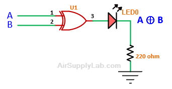
| Unit | Chip | VCC Pin | GND Pin |
|---|---|---|---|
| 1 | 7486 (XOR) | 14 | 7 |
Exp #4.1.1 Circuit Connection for On-Campus Lab
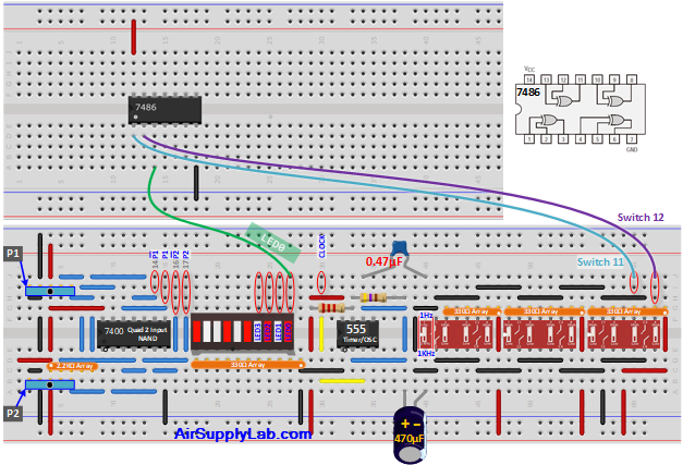
In this diagram, there is one chip (Unit 1 or U1) which is a 7486. The power and ground table has the unit number, the chip type, the power (VCC) pin, and the ground (GND) pin information. Insert the 7486 into the breadboard and connect the power pin (pin 14) to VCC (+5V) and the ground pin (pin 7) to GND (0V). Then connect a switch 11 from the array of switches to pin 1 of U1, switch 12 to pin 2 of U1, and pin 3 of U1 to an LED from the LED bar graph.
Question
- Build the circuit and verify that it produces the same results as given in the truth table for A ⊕ B. Change the Switch 11 and Switch 12 values, then record your observation in your report.
A
(Switch 11)B
(Switch 12)A ⊕ B
(LED0)0 (Down) 0 (Down) 0 (Down) 1 (Up) 1 (Up) 0 (Down) 1 (Up) 1 (Up)
Exp #4.1.1 Circuit Connection for Online Lab
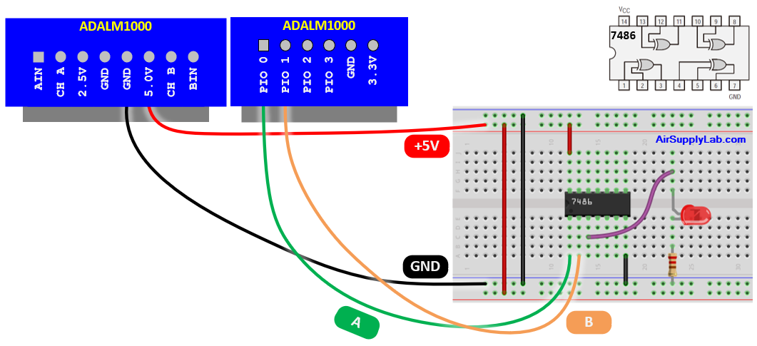
In this diagram, there is one chip (Unit 1 or U1) which is a 7486. The power and ground table has the unit number, the chip type, the power (VCC) pin, and the ground (GND) pin information. Insert the 7486 into the breadboard and connect the power pin (pin 14) to VCC (+5V) and the ground pin (pin 7) to GND (0V). Then connect PIO 0 from the ADALM1000 device to pin 1 of U1, PIO 1 to pin 2 of U1, and pin 3 of U1 to an LED.
Question
- Build this circuit and verify that it produces the same results as given in the truth table for A ⊕ B.
- Plug the ADALM1000 device into your computer, launch ALICE DeskTop program, and configure the digital I/O as shown below:
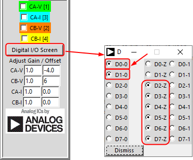
- The state of the PIO 0 pin on the ADALM1000 device can be controlled by the D0 value setting in the Digital I/O Screen window. Change the D0 and D1 values, then record your observation in your report.
B
(PIO 1)A
(PIO 0)A ⊕ B
(LED)0 0 0 1 1 0 1 1 - Take a photo of your circuit connection on the breadboard, and paste it into your report.
- Plug the ADALM1000 device into your computer, launch ALICE DeskTop program, and configure the digital I/O as shown below:
Here is the wiring diagram for the logic function AB + AB:
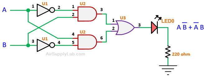
This circuit has three chips, U1 is a 7404 (Inverter), U2 is a 7408 (AND), and U3 is a 7432 (OR). Line up these chips along the same section of the breadboard, all facing the same way. Leave some space between them in case one of them is faulty and has to be extracted.
For each chip connect the power pin (pin 14) to VCC (+5V) and the ground pin (pin 7) to GND (0V). Next, connect all of the wires as shown in the wiring diagram. For example, connect pin 2 of U1 to pin 1 of U2. To keep track of which connections have been made, after you connect two pins with a wire, place a small checkmark on that wire in the wiring diagram. It is also a good idea to place a checkmark next to pin 14 and pin 7 in the power and ground table after you connect each to VCC and GND, respectively.
Exp #4,1.2 Circuit Connection for On-Campus Lab
Draw the wiring for the XOR gate circuit in the following diagram.

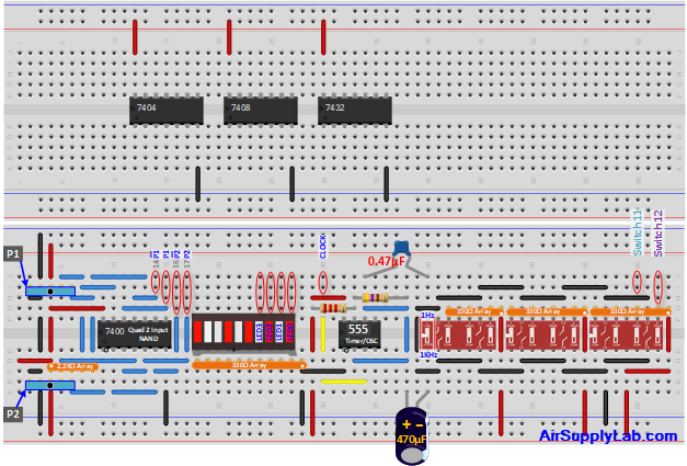
Question
- Build this circuit and verify that it produces the same results as given in the truth table for AB + AB.
- Draw the wiring diagram of the breadboard in your report.
- Record the observation and take a photo of your circuit connection on the breadboard, paste them in your report.
B
(PIO 1)
(Switch 12)A
(PIO 0)
(Switch 11)AB + AB
(LED0)0 0 0 1 1 0 1 1
Note: there is a problem drawing wiring diagrams as discussed above. You must constantly refer to the KB03: TTL IC Specifications or else go online to find each chip's pin numbers and then to place them in your drawing. Instead, you can use a circuit-drawing program called KiCad. (SCH stands for "schematic", meaning a circuit diagram). It allows you to place and connect symbols for gates and chips in your diagram that contain all pin numbers plus Vcc and ground (so a Vcc-ground table is no longer needed).
Once you draw a circuit with this tool, it is all right there. (You may want to print it out so you can check off connecting wires as you install them.) The program is available on the lab PC's plus you can download it from the web for free. Refer to the KB04: KiCad Tutorial for all instructions on how to download it to your computer and how to use it. It is of real benefit when wiring up your circuit to have your diagram on the PC screen, complete with pin and U (unit) numbers.
Exp #4.2 Debugging Your Circuit
Rarely will a circuit work the first time it is built? Inevitably there will be mistakes, also known as "bugs", either due to incorrect design or a mistake during wiring. In order to find the mistake, you need to troubleshoot or "debug" your circuit. For a combinational logic circuit here are some steps to debugging a circuit:
Steps for troubleshooting (debugging) a combinational logic circuit:
- Determine whether or not the circuit generates the correct outputs for all possible input combinations. If so, the circuit works properly. If not, record the input combinations that generate incorrect outputs. (The number of inputs can not be too high, else too many combinations to test.)
- For one of the input combinations that physically produced an incorrect output, shown on the diagram what the correct input and output of each gate should be (internal gates as well as the
final output). - Now, set the inputs to the circuit equal to that input combination. Note that while debugging a circuit it is best to manually control the inputs by connecting them to switches, or digital output pins from the ADALM1000 device, or by driving the 7493 counter with a manually clock signal.
- Using the logic probe, start from the output of the circuit and trace the values backward through the various components until you identify an incorrect value (a value that differs from the one you determined in step 2).
- Identify and fix the bug.
- Repeat steps 1 through 5 until there are no bugs remaining in the circuit.
There are two keys to being successful in troubleshooting your design. First, you must understand how your circuit is supposed to behave. Also, you need to have a good understanding of the behavior of each logic gate, hence the importance of Lab 3.
The circuits shown in the following debugging session have been drawn using KiCad. Notice how gates from different chips show different U numbers and how pin numbers are included automatically. Once you are familiar with KiCad, you'll see how much more efficient it is to draw your circuits.
- Let us experiment with debugging a circuit. First, this assumes that you have already built and tested the AB + AB circuit from Exp #4.1 (above) and have verified that it works properly. If it does not, you can use the following debugging steps to try to fix it.
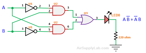
Figure 4.8.1: Correct XOR Circuit
- Suppose the bug in your circuit is due to the fact that instead of connecting the wire from U2 pin 4 to A, you connected it to U1 pin2, as shown below. (A fairly easy mistake to make.)
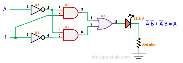
Figure 4.8.2: Circuit with Error
Debugging steps:
Step 1: with the bug, the circuit will generate the output values shown in the following truth table under Actual Value, instead of the correct values shown under A ⊕ B. There are two input combinations that generate the incorrect results shown in bold. From the values in the Actual Value column, it shows that the expression for the output of the circuit is now just A.
| A | B | A ⊕ B | Actual Value |
|---|---|---|---|
| 0 | 0 | 0 | 1 |
| 0 | 1 | 1 | 1 |
| 1 | 0 | 1 | 0 |
| 1 | 1 | 0 | 0 |
Step 2: for input combination, 00, the correct output value should be 0, but a check with your logic probe at the output of U3 (OR) will show it is 1. We start troubleshooting (debugging) by working backward from the output gate using the logic probe. The triangular symbols (red=1, green=0) represent the LED indicators on the logic probe. As you proceed, record the 1 and 0 values on your diagram.
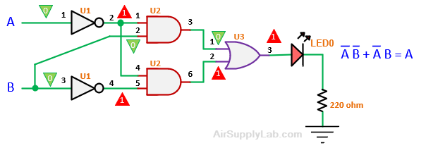
Figure 4.9: Circuit with Error, Output Becomes just A
- We first check the input pins of the OR. If the OR output is 0, then its inputs, pins 1 and 2, should both be 0's. The input at pin 1 turns out to be 0, as expected, so it's OK. But the input at pin 2 is a 1, which explains why the output of the OR is also 1 (i.e. 0 + 1 = 1). Since pin 1 is OK, we will ignore the upper half of the circuit and focus instead on the bottom half to see why the input to pin 2 is wrong.
- Now, if pin 2 of the OR is properly connected to pin 6, as the diagram shows, then the AND output will also be a 1. But an AND output of 1 implies that both its inputs, pins 4 and 5, must be 1's (output = 1 • 1 = 1), and the logic probe should show that they are.
- That pin 5 is a 1 is expected since B is the complement of B (0). On the other hand, we find pin 4 to be 1 even though it is supposed to connect directly to A (0). If we follow the wire from pin 4, we find that it ends, not at A but at A, the output of the upper inverter. We have located the bug. The circuit output is, therefore, AB (from lower AND) + AB (from upper AND) = A (B + B) = A, as the above truth table indicates.
Alternative debugging method
Assuming there are no electrical (as opposed to logic) problems with your circuit, problems like a bad chip, or one with no connection to Vcc or ground, or a broken wire, the following approach may save time since it doesn't involve poking around inside the circuit with a logic probe as in the previous example. It just requires adding a column to the original truth table with output values found when testing the actual circuit. We'll use the table for the XOR circuit shown at the top of the previous page to illustrate this.
| A | B | A ⊕ B | Actual Value |
|---|---|---|---|
| 0 | 0 | 0 | 1 |
| 0 | 1 | 1 | 1 |
| 1 | 0 | 1 | 0 |
| 1 | 1 | 0 | 0 |
The 1's in the Actual Values column lie in the first two rows where A = 0. So we could say that the circuit output is simply A. But this implies a circuit with no AND and OR gates — very different from the XOR circuit. In order to compare the two, we want the same structure for each (i.e. two inverters, two ANDs, and an OR). So, instead, we write separate AND expressions (product terms) for the first and second rows in the Actual Values column and combine them as shown:
Actual output = A B + A B
XOR output = A B + A B
We can see right away that the problem is the underlined A which should be A. In other words, the wire into pin 4 of the lower AND should come directly from the A and not from the output A of the upper Inverter. Problem solved.
Exp #4.3 * Three-Inputs Voter Circuit
A majority voter is a circuit with three inputs that we will refer to as A, B, and C. It has one output which we will refer to as V. The value of V will agree with the majority value on the inputs. Thus, if the majority (two or more) of the values are 0, V will be 0. If the majority of the values are 1, V will be 1. Given this definition of the majority voter, complete the truth table below for V, and record it in your report.
| A | B | C | V |
|---|---|---|---|
| 0 | 0 | 0 | |
| 0 | 0 | 1 | |
| 0 | 1 | 0 | |
| 0 | 1 | 1 | |
| 1 | 0 | 0 | |
| 1 | 0 | 1 | |
| 1 | 1 | 0 | |
| 1 | 1 | 1 |
Let's think about this circuit. If two or three inputs are 1, output V will be 1. Otherwise, it will be 0. Verify that your values for V in the truth table agree with this definition. If so, then we can determine a logical expression for V; i.e. V = AB + BC + AC. We can verify that this is correct by showing that the truth table for V and for AB + BC + AC are the same. Complete the truth table below to prove that these two functions are the same, and record it in your report.
| A | B | C | V | AB | BC | AC | (AB + BC) + AC |
|---|---|---|---|---|---|---|---|
| 0 | 0 | 0 | |||||
| 0 | 0 | 1 | |||||
| 0 | 1 | 0 | |||||
| 0 | 1 | 1 | |||||
| 1 | 0 | 0 | |||||
| 1 | 0 | 1 | |||||
| 1 | 1 | 0 | |||||
| 1 | 1 | 1 |
Question
- Build this circuit and verify that it produces the same results as given in the truth table for V:
- Draw the logic diagram for V = AB + BC + AC. Mark the chip numbers and pin numbers on all logic gates in the diagram. (Check the diagrams in Exp #4.2)
- Implement the circuit and verify that it behaves correctly. If it does not, use the debugging steps in Exp #4.2 to troubleshoot your design. Take a photo of your circuit connection on the breadboard, and paste it into the report.
Exp #4.4 * Debug Your Circuit (For On-Campus Lab Only)
Assuming that you were lucky and wired your circuit properly, you haven't had a chance to practice your debugging skills. In this section, you will each take turns inserting a bug for your partner after which your partner will troubleshoot the circuit. Follow the steps shown in Exp #4.2 to debug your circuit. Document your process as shown in Exp #4.2 in your lab journal. Demonstrate your debugging technique to your instructor.


