Serial Peripheral Interface Bus (SPI)
SPI (Serial Peripheral Interface Bus) is a high-speed, synchronous serial communication bus widely used in embedded systems. It supports full-duplex (4-wire mode), fast data transfer rates, and a simple master–slave structure..
Used in:
- Flash memory (W25Q series)
- ADC/DAC
- IMU sensors
- LCD/OLED/TFT displays
- Real-time clocks
- FPGA communication
Interface and Features
SPI features include:
- SPI signals include:
- SCLK: Serial Clock (output from master)
- MOSI: Master Output Slave Input (data output from master)
- MISO: Master Input Slave Output (data output from slave)
- /SS: Slave Select (often active low, output from master)
- SDAT: Serial Data I/O (bidirectional I/O, combined MOSI and MISO signals together)
- Data length: 3- to 16-bit data width
- Bit rate: supports up to 18 Mbps
- SPI serial bus can be configured as 4-wire (default) and 3-wire mode
SPI Clock Modes (CPOL + CPHA)
SPI has no pre-defined protocol, so the master and slave must agree on the data frame for the exchange. The data frame is described by clock polarity (CPOL) and clock phase (CPHA). The CPOL parameter defines whether the clock is idle when high or low. The CPHA parameter is used to shift the sampling phase. If CPHA = 0, the data will be sampled on the leading (first) clock edge. If CPHA = 1, the data are sampled on the trailing (second) clock edge, regardless of whether that clock edge is rising or falling. The 4 modes combine polarity and phase according to the following table:
Table: SPI Clock Phase (CPHA) and Clock Polarity (CPOL) Operation
| Mode | Clock Polarity (CPOL) |
Clock Phase (CPHA) |
SCLK Transmit Edge | SCLK Receive Edge | SCLK Idle State |
| 0 | 0 | 0 | Falling | Rising | Low |
| 1 | 0 | 1 | Rising | Falling | Low |
| 2 | 1 | 0 | Rising | Falling | High |
| 3 | 1 | 1 | Falling | Rising | High |
CPOL: used for clock idle state
- 0 — Clock idle low level
- 1 — Clock idle high level
CPHA: used to shift the sampling phase
- 0 — Data Sampled at the leading edge (no delay)
- 1 — Data Sampled at the trailing edge (delay)
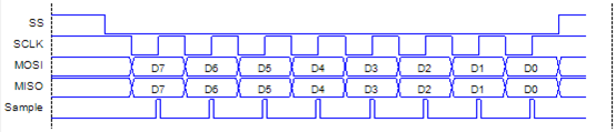
Timing Diagram for Clock Polarity and Phase
Timing Diagram for Clock Polarity and Phase
The following diagram illustrates the four possible states of these parameters and the SPI mode.
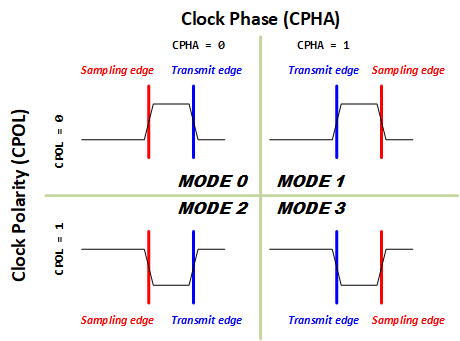
- Mode 0 — CPOL = 0, CHPA = 0
Data is sampled at the leading rising edge of the clock. The data must be available before the first clock signal rises. The clock idle state is low (0). The data on MOSI and MISO lines must be stable while the clock is high and can be changed when the clock is low. The data is captured on the clock's rising transition and propagated on the falling clock transition. Mode 0 is the most common mode for SPI bus slave communication.
- Mode 1 — CPOL = 0, CHPA = 1
Data is sampled at the trailing falling edge of the clock. The first clock signal rising can be used to prepare the data. The clock idle state is low (0). The data on MOSI and MISO lines must be stable while the clock is low and can be changed when the clock is high. The data is captured on the clock's falling transactions and propagated on rising clock transactions.
- Mode 2 — CPOL = 1, CHPA = 0
Data is sampled at the leading falling edge of the clock. The data must be available before the first clock signal falls. The clock idle state is high (1). The data on MOSI and MISO lines must be stable while the clock is low and can be changed when the clock is high. The data is captured on the clock's falling transition and propagated on the rising clock transition.
- Mode 3 — CPOL = 1, CHPA = 1
Data is sampled at the trailing rising edge of the clock. The first clock signal falling can be used to prepare the data. The clock's idle state is one. The data on MISO and MOSI lines must be stable while the clock is high and can be changed when the clock is low. The data is captured on the clock's rising transition and propagated on the falling clock transition.
SPI Bus Connection Modes
SPI has two common wiring modes: 4-wire (standard full-duplex) and 3-wire (half-duplex). Both follow the SPI master-slave protocol, but they differ in wiring, performance, and use cases.
4-Wire SPI (Standard Full-Duplex Mode)
4-wire serial bus mode: SCLK, MOSI, MISO, AND SS signals
| Signal | Direction | Description |
| SCLK | Master → Slave | Serial Clock |
| MOSI | Master → Slave | TX From Master |
| MISO | Slave → Master | RX From Slave |
| CS/SS | Master → Slave | Chip Select/Slave Select (active low) |
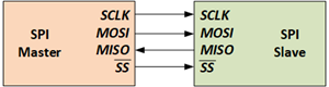
4-wire bus mode is the SPI standard connection mode. It supports full-duplex data transactions, which means SPI allows transmitting and receiving data simultaneously on two data lines (MOSI and MISO),
3-Wire SPI (Half-Duplex Mode)
3-wire serial bus mode: SCLK, SDAT, and SS signals
| Signal | Direction | Description |
| SCLK | Master → Slave | Serial Clock |
| SDAT | Bidirectional | Combined MOSI + MISO |
| CS/SS | Master → Slave | Chip Select/Slave Select (active low) |
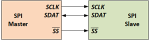
In 3-wire serial bus mode, MOSI and MISO lines are combined into a single bidirectional data line (SDAT). Transactions are half-duplex to allow for bidirectional communication. Reducing the number of data lines and operating in half-duplex mode also decreases the maximum possible throughput; many 3-wire devices have low-performance requirements and are instead designed with low pin count in mind.
Comparison Between 4-Wire SPI and 3-Wire SPI
SPI has two common wiring modes: 4-wire (standard full-duplex) and 3-wire (half-duplex).
Both follow the SPI master-slave protocol, but they differ in wiring, performance, and use cases.
- Signal Comparison
Feture 4-Wire SPI 3-Wire SPI Clock SCLK SCLK TX Line MOSI SDIO (shared) RX Line MISO SDIO (shared) Chip Select CS/SS CS/SS Number of data lines 2 (one TX, one RX) 1 shared data line Minumumwire 4 wires 3 wires Master-slave roles TX & RX independent One pin must switch direction - Duplex Mode
Feture 4-Wire SPI 3-Wire SPI Duplex Mode Full-duplex Half-duplex Send and receive at the same time ✔ Yes ✘ No One clock transfers 2 bits exchanged (1 in, 1 out) 1 bit transferred - Communication Behavior
✔ 4-Wire SPI
- MOSI → Master sends data
- MISO → Slave sends data
- Both happen simultaneously
- Ideal for high-bandwidth devices
✔ 3-Wire SPI- SDIO line used for both TX and RX
- Master must switch SDIO direction (output → input)
- Transmission occurs in two phases:
- Master → Slave
- Slave → Master
- Requires tri-state logic and strict timing control
- Speed & Performance
Feture 4-Wire SPI 3-Wire SPI Maximum speed Highest Medium-High Full-duplex throughput 2× higher 1× only Turn-around delay None Required (switch direction) Efficiency Very high Lower due to direction switching - Hardware Complexity
Feture 4-Wire SPI 3-Wire SPI Hardware Simple More complex (bidirectional buffer) Master direction control Not required Mandatory Slave tri-state control Only for MISO Required for SDIO PCB routing Needs more pins Fewer pins, simpler routing - Use Cases
✔ 4-Wire SPI – Common in:
- High-speed sensors
- SPI Flash (W25Q series)
- High-resolution displays (ILI9341)
- Fast ADC/DAC
- When full-duplex is required
- MCU-to-FPGA communication
✔ 3-Wire SPI – Common in:- Small LCD controllers (ST7789 SPI mode)
- Touch controllers
- Low-pin-count ICs (8-pin packages)
- EEPROMs or configuration memories
- Cost-sensitive designs
- Small MCUs with limited I/O pins
- Advantages & Disadvantages
✔ 4-Wire SPI Advantages
- Fastest performance
- Full-duplex
- Most compatible with commercial devices
- No pin switching required
- Best for high-bandwidth applications
✔ 4-Wire SPI Disadvantages- Requires more pins
- More PCB traces
- Not suitable for tiny IC packages
- More GPIO usage for multi-slave systems
✔ 3-Wire SPI Advantages- Saves 1 data pin (important for small MCUs)
- Less PCB routing complexity
- Still much faster than I2C
- Useful for cost/pin-constrained devices
✔ 3-Wire SPI Disadvantages- Half-duplex only
- Lower data throughput
- More difficult to implement
- Requires tri-state switching
- More protocol-level overhead
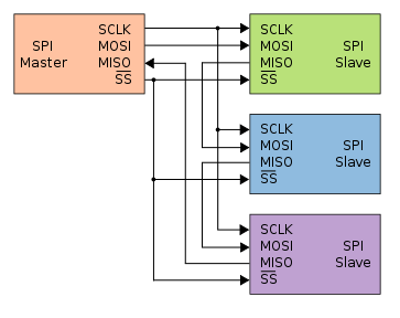
SPI Connections for Multiple Slaves
SPI devices communicate in full-duplex mode using a master-slave architecture with a signal master. There are two ways to connect multiple slaves with a master:
Individual Slave Select Configuration
Shared SPI Bus + Individual Chip Select Lines (Most Common)
In this configuration, the SCLK, MOSI, and MISO are shared by all devices. Each device has an individual slave select (/SS) line. The master will pull low on a slave /SS line to choose a device for communication. A pull-up resistor on the /SS line is highly recommended for each device to reduce crosstalk between devices. The data lines (MOSI and MISO) are connected to the slaves in parallel.
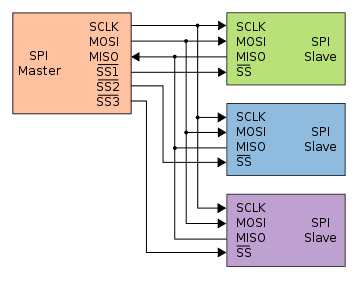
✔ Rules:
- Only one CS is LOW at a time
- Non-selected slaves MUST tri-state MISO
- All slaves must support the same voltage level
- SCLK/MOSI/MISO are shared
✔ Pros:
- Simple
- Most widely supported
- Maximum speed
✔ Cons:
- Requires many CS pins
(N devices → N extra GPIOs)
Use a decoder (e.g., 74HC138, 74HC154) to reduce GPIO usage.
3 GPIO Pins → 8 CS/SS lines
✔ Pros:
- Saves GPIO pins
- Supports many devices
✔ Cons:
- Adds hardware
- Slight propagation delay
SPI Daisy-Chain Mode
SPI Daisy-Chain Mode
SPI devices may be connected in a daisy chain configuration. The data lines (MOSI and MISO) are connected with slaves in a serial connection — the first slave's data output is connected to the second slave's data input, etc. The entire chain functions as a communication shift register; daily chaining is often accomplished with shift registers to provide a block of inputs or outputs via SPI. This configuration requires only a single /SS line from the master, rather than a separate /SS line for each slave.

✔ Requirements:
- Devices must support daisy chaining (not all do)
- Common in drivers like MAX7219, shift registers, and LED drivers
✔ Pros:
- Only one CS pin is needed
- Very clean wiring
✔ Cons:
- Slaves must be designed for shift-register chaining
- Latency increases with each chained device
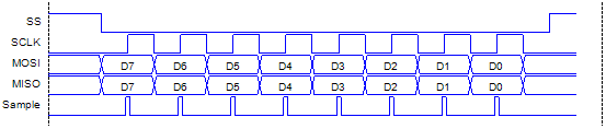
How SPI Transfers Data Between Master and Slave
How SPI Transfers Data Between Master and Slave
SPI communication is a synchronous, serial, full-duplex protocol in 4-wire mode. Data transfer is driven entirely by the Master, which controls the clock, the transaction timing, and the activation of each Slave device.
- Master Selects the Slave (CS/SS Activation)
- Each slave device has a Chip Select (CS or SS) input.
- The Master begins a transfer by driving the selected slave’s CS line LOW.
- All other slaves must keep their MISO outputs tri-stated (Hi-Z).
Only the slave with CS = LOW is allowed to respond.
- Master Generates the Clock (SCLK)
SPI uses a synchronous clock.- The Master is the only device that generates SCLK.
- Slaves never drive the clock.
- Frequency (e.g., 1 MHz, 10 MHz, 40 MHz…)
- Polarity (CPOL) → idle level of the clock
- Phase (CPHA) → sampling edge
- Both Master and Slave must use the same CPOL/CPHA mode (Mode 0–3)
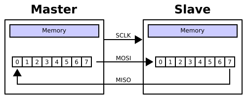
In SPI, the master and slave each contain a shift register, and together they operate as a synchronized circular buffer, exchanging data simultaneously on every clock pulse.
- Shift Register Operation (Core of SPI)
SPI transfers data using synchronous shift registers inside the Master and Slave.
How it works (bit-level):- Both Master and Slave have an internal shift register.
- On each SCLK edge:
- Master shifts out 1 bit on MOSI
- Slave shifts out 1 bit on MISO
- Each side samples the incoming bit at the defined CPHA sampling edge
This is why SPI is full-duplex in 4-wire mode.
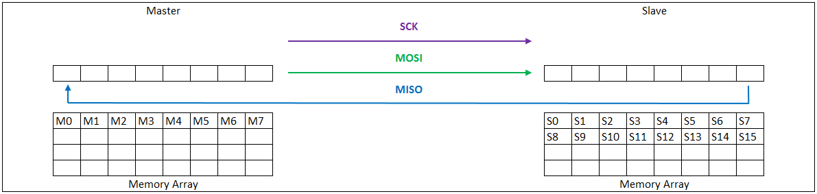
- One Clock Pulse = One Bit Transferred
On each clock cycle:- Master → Slave (via MOSI): 1 bit
- Slave → Master (via MISO): 1 bit
If transferring 8 bits:- 8 clock pulses are required
- Both Master and Slave shift and sample 8 bits
- Both sides end with a completed data byte
- Transaction Example (8-bit Transfer)
Step-by-step:- Master pulls CS low
Slave is now active. - Master outputs clock signals
For each SCLK edge:- Master shifts MOSI → Slave
- Slave shifts MISO → Master
- Both devices read incoming bits
Depending on CPHA:- A rising or falling edge is used for sampling
- The opposite edge is used for data setup
- After 8 clocks (1 byte)
- Master’s shift register contains Slave’s byte
- Slave’s shift register contains the Master’s byte
- Master may continue clocking
To transfer more bytes. - Master pulls CS high
Transaction ends.
Slave tri-states its MISO line.
- Master pulls CS low
- Full-Duplex Behavior
Even if the master only wants to read data, SPI STILL REQUIRES sending dummy bytes.
Example: To read a Flash chip:- Master sends 0x00 or 0xFF on MOSI
- Slave outputs real data on MISO
- Master ignores the MOSI data and captures MISO data
- 1 TX bit + 1 RX bit per clock
- Half-Duplex (3-Wire Mode) Variation
In 3-wire SPI:- MOSI and MISO are merged into SDIO
- Master must switch SDIO direction:
- Output mode during transmit
- Input mode during receive
- End of Transfer
A transfer ends when:- Master completes the required number of clock cycles
- Master drives CS high
- Slave:
- Stops driving MISO
- Updates any internal state depending on the command
- Returns to idle mode
Summary of SPI Data Flow
| Phase | Description |
| 1. CS Low | Master select slave |
| 2. Clock Starts | Master generates SCLK |
| 3. Bit Shifting | MOSI/MISO exchanged per clock edge |
| 4. Byte Complete | Shift registers updated |
| 5. More Bytes? | Master continues clocking |
| 6. CS High | Slave deselected, MISO Hi-Z |
Summary Table — When to Choose Which?
| Requirement | Best CHoice |
| Highest speed | 4-Wire SPI |
| Full-duplex needed | 4-Wire SPI |
| MCU has many GPIOs | 4-Wire SPI |
| Low-pin-count design | 3-Wire SPI |
| Display controllers that use SDI/SDO | 3-Wire SPI |
| Daisy-chain LED drivers | 4-Wire SPI |
| Cost-sensitive design | 3-Wire SPI |
| High data throughput | 4-Wire SPI |
Conclusion
4-Wire SPI is faster, simpler, and offers full duplex, making it ideal for high-performance applications.
3-Wire SPI reduces pin count and PCB complexity but introduces half-duplex constraints and requires careful control of the shared SDIO line.
Both modes follow the SPI protocol but are optimized for different hardware design priorities:
-
- 4-Wire = Performance & Simplicity
- 3-Wire = Pin Saving & Compact Design
-
To write code for a new SPI device, you need to note a few things:
- What is the maximum SPI clock speed the device can use?
- Is data first shifted in the Most Significant bit (MSb) or the Least Significant bit (LSb)?
- Is the data clock idle when high or low? Are samples on the rising or falling edge of clock pulses?
- Is the connection in 4-wire or 3-wire mode?
Reference:
-
- Wikipedia https://en.wikipedia.org/wiki/Serial_Peripheral_Interface_Bus
- DLNWare - SPI http://dlnware.com/theory/SPI-Bus
- CORELIS - SPI Interface https://www.corelis.com/education/SPI_Tutorial.htm
-