Analog-to-Digital Converter (ADC or A/D Converter)
The signals of the natural environment, such as voice, temperature, light ... and so on, are continuous-time and continuous-amplitude variable (analog) signals. Analog signals have infinite states available. But, the computers we are using are digital signal systems. Digital signals have two states — on (1) or off (0). The analog signals need to be converted into a digital representation which can then be stored in a computer for further processing. An A/D Converter is a device that converts analog signals (usually voltage) obtained from environmental phenomena into digital format. In other words, ADC digitizes an analog signal by converting data with infinite states to a series of pulses. The amplitudes of these pulses can only achieve a finite number of states.
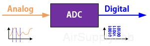
Figure 1: Basic Function of ADC
ADCs have the following key characteristics:
- Input range, or Full-Scale input Range, measured in Volts, is the range of voltages that can be applied at the input of the ADC.
- Output range, or quantization, measured in bits, is the number of bits in each output sample (typical values are 8, 12, 16, 24, and 32). It is common to say an "8-bit ADC", meaning an ADC with output samples that are 8-bit wide.
- The sampling rate, measured in Hz, is the rate at which the ADC generates its output samples.
ADC Specifications
Full-Scale Input Range
The full-scale input of an ADC is the largest signal amplitude that can be delivered to the converter before the signal is clipped in its digital output representation.
Sampling Rate (fs)
The sampling rate is the frequency expressed in Hertz (Hz) at which the ADC samples the input analog signal.
The Nyquist Theorem (or Shannon Theorem) states that an analog signal with the highest frequency of fa MUST be sampled at a sampling rate fs > 2 fa to avoid loss of information.
- If fs < 2 fa then phenomena called aliasing will occur in the analog signal bandwidth.
Resolution
There are two types of resolution in the A/D Conversion: bit-resolution and voltage-resolution.
- The bit resolution of an ADC refers to the number of bits in the digital output code of the ADC.
- The voltage resolution is the minimum change in input voltage which can be resolved by the ADC. It is the same as analog quantization size.
Voltage-Resolution, (or Quantization, Least Significant bit Voltage)
The voltage resolution represents the minimum change in voltage that is required to guarantee a change in the output code level. It is also called the least significant bit voltage. The quantization of ADC (Q) is equal to the voltage resolution (or the LSB voltage).
The voltage resolution of an ADC is equal to its overall voltage measurement range divided by the total numbers of digital output:
ResolutionVoltage = Q = VLSB = (VRef,max - VRef,min) / 2n = VFSR / 2n -------- (1)
If you are using an 8-bit ADC, and the voltage input range of the ADC is from 0 to 5 volts. An 8-bit digital value can represent 256 (28 = 256) different numbers. In this example, the bit-resolution of the ADC is 8-bit, and it has a voltage resolution of 20mV (10v/256).
The Ideal Transfer Function for A/D Conversion
The transfer function of an ADC is a plot of the voltage input to the ADC versus the code's output by the ADC. The horizontal axis represents a continuous analog input signal. The vertical axis shows the digital output codes which can be thought of as a level for rounding off the analog input signal to its nearest digital equivalent. The full-scale input range of the ADC is equally divided over the total number of digital output codes to transform the dashed red line into the staircase blue line as shown in Figure 2.
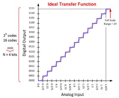
Figure 2: Ideal Transfer Function of a 4-bit ADC
The number of bits is the number of binary digits in the digital output code used to represent the full-scale analog signal. In this example, we have 4-bit or binary digits ADC, so N = 4, and the number of codes here is 24 = 16, which corresponds to counting from binary 0000 to 111 which is 0 to 15 in decimal, Here, we assume the output of the ADC is linear.
- N: the number of bits ADC
- VFSR: the Full-Scale input Range of the ADC
- VLSB: the minimum resolvable voltage, or ADC voltage resolution
$\begin{array}{lllllllllllllll} {NumberofCodes = {2^N}}\\ {Resolutio{n_{bit}} = N}\\ {Resolutio{n_{Voltage}} = Q = {V_{LSB}} = \frac{{{V_{FSR}}}}{{{2^N}}}} \end{array}$
The full-scale input range in this example is 2V (0 to 2 V). The voltage resolution is often identified as the width of the least significant bit, it can be computed by taking the full-scale range and dividing by the total number of bits, or 2 to the N power. Therefore, the least significant bit width or voltage resolution can be calculated by dividing 2V by 16 to get a resolution of 0.125V.
$N = 4$
${V_{FSR}} = 2V - 0V = 2V$
${V_{LSB}} = \frac{{{V_{FSR}}}}{{{2^N}}} = \frac{{2V}}{{{2^4}}} = 0.125V$
The full-scale range in this example is 2V, but the maximum detectable input voltage is the full-scale range minus one LSB or 1.875V in this example.
Math Conversion Equations
The A/D Converter samples the analog signal and then provides a quantized digital code to represent the input signal. The digital output codes get post-processed and results can be reported to an operator who will use this information to make decisions and take actions. Therefore, it is important to correctly relate the digital codes back to the analog signals they represent.
In general, the ADC input voltage is related to the output code by a simple relationship, as shown in Equation 1:
${V_m} = {D_{out}} \times {V_{LSB}}$ ---------- (2)
where Vm (V) is the ADC's input voltage or the measured voltage; Dout is the ADC's digital-output code in decimal format, and VLSB is the voltage resolution or the value of the least significant bit in the ADC code.
Equation 1 is a general equation that can work for any ADC. It doesn't matter if the ADC's output code is in straight binary or two's complement format, as long as the binary number is correctly converted to its equivalent decimal value.
Example 1
The 68HC11 microcontroller has an 8-bit A/D Converter, and the full-scale input range is 0 to 5.12V.
- The VFSR of the 68HC11 is
VFSR = 5.12V - 0V = 5.12V - The voltage resolution is
VLSB = VFSR / 28 = 5.12V / 256 = 0.2031 V = 20.3 mV, which means the input change of 20mV changes LSB
Q1: If the input voltage is 2.56V, what is the converted digital value?
Dout = Vm / VLSB = 2.56V / 20mV = 128
Converting the Dout to binary gives (1000 000)2 or 0b1000 0000, which will be stored in the ADC result register
Q2: If the ADC reading is 165, what is the input voltage?
Vm = Dout × VLSB = 165 × 20mV = 3300 mV = 3.3 V
Example 2
A DC voltmeter is rated at 14-bit resolution and has a full-scale input range of ± 5V. Assuming the meter's ADC is ideal, what is the quantization value?
A.
VFSR = (5 V - (-5 V) ) = 10 V
Q = VFSR / 2n = 10 V / 214 = 0.61 mV
Example 3
Consider a thermocouple giving an output of 0.5 mV/ºC. What will be the bit-resolution required when its output passes through ADC; if temperatures of 0 ~ 200ºC are to be measured with a resolution of 0.5ºC.
A:
Full scale output voltage from the thermocouple = (200 ºC - 0 ºC) x 0.5 mV/ºC = 100 mV
The voltage resolution is 100 mV / 2n. For a resolution of 0.5 ºC, the ADC must be able to detect a signal from the sensor of: 0.5 ºC x 0.5 mV/ºC = 0.25 mV
0.25 mV is the smallest input value that can produce a 1-bit change in the ADC output. It is the voltage resolution value of ADC.
So, voltage resolution = 0.25 mV = 100 mV / 2n → n = 8.6, thus 9-bit of ADC is required.
From here, it is necessary to look at specific ADC architectures in order to determine the best ADC for the job. This includes:
- SAR (Successive Approximation Register) ADCs
- Flash ADCs
- Delta-Sigma ADCs
SAR ADC
SAR ADC is the most commonly used method. It has a smaller chip area and lower power consumption analog-to-digit conversion. It is frequently the architecture of choice for medium-to-high-resolution applications with sample rates under 5 mega samples per second (MSPS). Bit resolution for SAR ADCs most commonly ranges from 8 to 16 bits. These features make the SAR ADCs especially suitable for the following applications:
- Wearable, handheld, and sensor devices
- Magnetic card reader
- High-speed data collection
- Power meter
- Pulse oximeter
SAR ADC Architecture
The SAR ADC basically implements a binary search algorithm. There are many variations for implementing a SAR ADC, but the basic architecture is simple. The SAR ADC circuit typically consists of four chief sub-circuits, and it is shown in Figure 3.
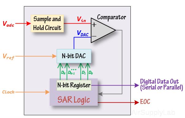
Figure 3: Simplified N-bit SAR ADC Architecture
- A sample and hold circuit to acquire the input analog voltage (Vadc).
- An analog voltage comparator that compares Vin to the output of the internal DAC (VDAC) and outputs the result of the comparison to successive approximate register (SAR logic).
- A successive approximate register subcircuit was designed to supply an approximate digital code for Vin to the internal DAC.
- An internal reference DAC that, for comparison with VREF, supplies the comparator with an analog voltage equal to the digital code output of the SAR logic.
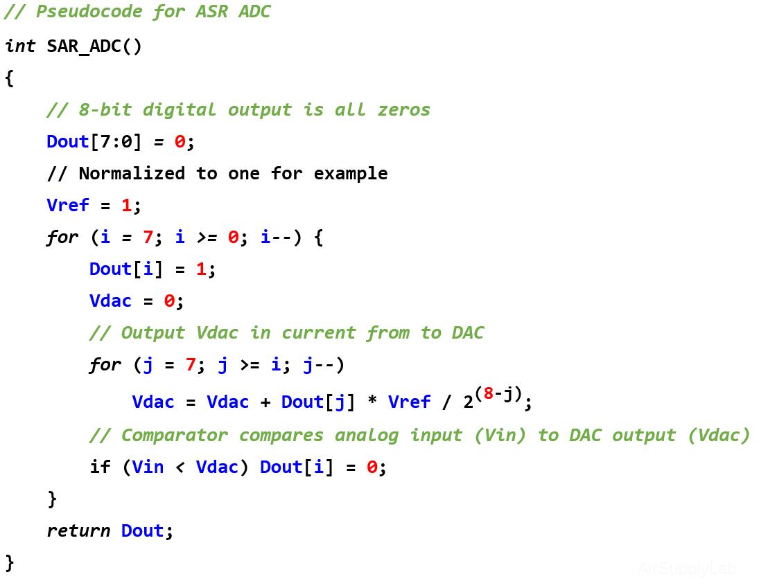
Basic Operation of the SAR ADC
The SAR ADC does the following steps for each sample:
- The analog input voltage (Vadc) is sampled and held.
- To implement the binary search algorithm, the N-bit register is first set the MSB to 1 (that is 1000 ... 002). This will set the DAC output (VDAC) to be Vref / 2, where Vref is the reference voltage provided to the ADC.
- A comparison is then performed to determine if Vin is less than, or greater than, VDAC.
- If Vin is greater than VDAC, the comparator output is logic 1, and the MSB of the N-bit register remains at 1.
- Conversely, if Vin is less than VDAC, the comparator output is a logic low and the MSB of the register is cleared to logic 0.
- The SAR control logic then moves to the next bit down, forces that bit high, and does another comparison. The sequence continues all the way down to the LSB.
- Once all bits have been approximated, the N-bit digital approximation is output at the end of the conversion (EOC).
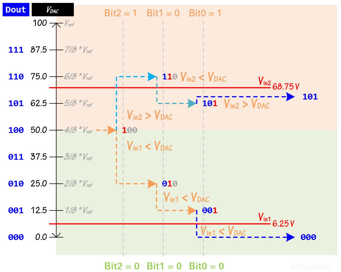
Figure 4: SAR Operation (3-bit ADC Example)
Figure 4 shows an example of a 3-bit conversion. The y-axis represents the VDAC voltage. Let us focus on the Vin1 = 6.25 V in the example, the first comparison sets the MSB of the register to 1002, and the comparison shows that Vin1 < (VDAC = Vref / 2). Thus, bit 2 is set to 0. The register is then set to 0102 and the second comparison is performed. As Vin1 < (VDAC = Vref / 4). Bit 1 is set to 0, and the register is then set to 0012 for the final comparison. Finally, bit 0 is set to 0 because Vin1 < (VDAC = Vref / 8). The digital result for Vin1 is 0002.
Notice that a 4-bit ADC requires three comparison cycles. In general, an N-bit SAR ADC will require N comparison cycles and will not be ready for the next conversion until the current one is complete. This explains why these ADCs are power - and space-efficient.
Flash ADC
A flash ADC (also known as a direct-conversion ADC) is a very fast type of ADC that uses a linear voltage ladder with a comparator at each "rung" of the ladder to compare the input voltage to successive reference voltages. For the n-bit A/D converter, 2n-1 separate voltage comparators are used in parallel, with each having the analog input voltage as one input. The resistor ladder steps down the reference voltage bit by bit and is applied as other input to each comparator.
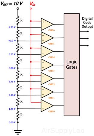
Figure 5: A 2-bit Flash ADC
Thus when the analog voltage is applied to ADC, all those comparators for which the analog voltage is greater than the reference voltage will give a high output and those below the reference will give a low output. The resulting output is fed in parallel to a logic gate system which translates them into a digital output register.
For example in Figure 5, if Vin = 6.00 V, then the first 4 comparators (CMP0 ~ CMP3) from the bottom will return a logic high signal while the top three (CMP4 ~ CMP6) will return a low signal to the logic gates. The logic gates will convert the input to binary (100)2.
The flash ADC has the following advantages and disadvantages:
- Advantages
- Very fast
- Disadvantages
- For lower-resolution ADC. Many comparators are required for higher-resolution ADC; ex. 8-bit flash ADC needs 28 - 1 = 255 comparators.
- Higher cost
Delta-Sigma ADC
The Delta Sigma Analog to Digital Converter provides a low-power, low-noise front end for precision measurement applications. It can be used in a wide range of applications, depending on the resolution, sample rate, and operating mode. For example, The Delta-Sigma ADC can produce 16-bit audio; high speed and low resolution for communications processing; and high-precision 20-bit low-speed conversions for sensors such as strain gauges, thermocouples, and other high-precision sensors. When processing audio information, the Delta-Sigma ADC is used in a continuous operation mode. When used for scanning multiple sensors, the Delta-Sigma ADC is used in one of the multi-sample modes. When used for single-point high-resolution measurements, the Delta-Sigma is used in single-sample mode.
Quiz
{quiz id=2}