Lesson 03: Power System
The PSoC 5LP microcontroller series is designed with a sophisticated power system featuring multiple internal regulators and separate supply pins for analog and digital components. This design enhances the efficiency and stability of the device's operation. Here's a detailed overview of the power systems in the PSoC 5LP:
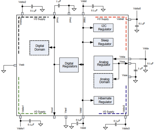
Figure 3.1: Power Domain Diagram
3.1 Dual-Rail Power Supply
Dual-Rail Power Supply:
Unlike many microcontrollers, the PSoC 5LP operates with separate external analog and digital supply pins:
- VDDA (Analog Supply Pin):
- This pin supplies the analog components of the microcontroller.
- It ensures that the analog circuits receive a stable and noise-free voltage, which is crucial for the accuracy and performance of these components.
- VDDD (Digital Supply Pin):
- This pin powers the digital core logic of the microcontroller.
- The separation from the analog supply helps to minimize digital noise affecting the analog circuits.
This separation ensures clean power delivery and minimizes noise interference between the digital and analog domains.
3.2 Internal Voltage Regulators
Internal Voltage Regulators:
PSoC 5LP boasts two internal 1.8V regulators:
- Analog Regulator (VCCA):
- Powers the analog domain within the microcontroller.
- Provides a stable power source for sensitive analog components like ADCs, DACs, and op-amps.
- Digital Regulator (VCCD):
- Supplies power to the digital core logic.
- Ensures stable operation of digital components like CPUs, memory, and digital peripherals.
The outputs of these regulators (VCCD and VCCA) have specific capacitor requirements, as detailed in the PSoC 5LP datasheet. These capacitors are essential for stabilizing the output voltage and filtering out noise, ensuring reliable operation of the microcontroller.
3.3 Supply for I/O Pins
Supply for IO/ Pins:
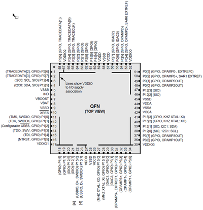
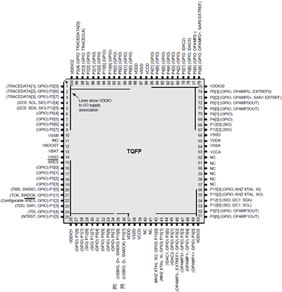
PSoC 5LP provides four VDDIO pins to power a specific set of I/O pins. Using the VDDIO pins, a single PSoC can support multiple voltage levels, reducing the need for off-chip level shifters. The black lines drawn on the pinout diagram in Figure 3.2 and Figure 3.2, as well as Table 3.1, show the pins that are powered by each VDDIO.
68-Pin QFN Part Pinout
100-Pin TQFP Part Pinout
Table 3.1: VDDIO and Port Pin Associations
| VDDIO | Port Pins |
|---|---|
| VDDIO0 | P0[7:0], P4[7:0], P12[3:2] |
| VDDIO1 | P1[7:0], P5[7:0], P12[7:6] |
| VDDIO2 | P2[7:0], P6[7:0], P12[5:4], P15[5:4] |
| VDDIO3 | P3[7:0], P12[1:0], P15[3:0] |
| VDDD | P15[7:6] (USB D+, D-) |
- VDDIO0/1/2/3: Independent I/O supplies. May be any voltage in the range of 1.8 to VDDA.
3.4 Specialized Regulators
Specialized Regulators for Diverse Needs:
Beyond the core digital and analog regulators, PSoC 5LP provides additional specialized power sources:
- Sleep Regulator: Active in sleep modes, this regulator manages power for domains that need to remain operational while the microcontroller is in a low-power state.
- I2C Regulator: Specifically powers the I2C logic, allowing for communication even when other microcontroller parts are powered down.
- Hibernate Regulator: Supplies keep-alive power during hibernate mode for state retention and quick recovery.
These specialized regulators offer flexibility and optimize power consumption for different operating modes and functionalities.
3.5 Boost Converter
Purpose:
- Generates a higher output voltage from a lower input voltage, allowing operation in applications with limited power sources (e.g., solar panels, single-cell batteries).
- Provides a minimum of 1.8V supply voltage, even when the input voltage is as low as 0.5V.
- Can be used to drive components requiring higher voltages than the main system supply (e.g., 5V LCD glass in a 3.3V system).
Required External Components:
- Inductor: Choose an inductor of 4.7 μH, 10 μH, or 22 μH. Optimize the value based on input voltage, output voltage, temperature, and current. Place the inductor within 1 cm of the VBAT and IND pins, ensuring a minimum saturation current of 750 mA.
- Schottky Diode: Use a Schottky diode with a forward current rating of at least 1.0 A and a reverse voltage of at least 20 V. Position it within 1 cm of the IND and VBOOST pins.
- Capacitors: Employ a 22 μF capacitor (CBAT) close to the VBAT pin for local bulk storage and regulator stability. A 22 μF bulk capacitor (CBOOST) should be connected near the VBOOST pin for regulator output stability. All capacitors must be rated for a minimum of 10 V.
Configuration and Operations:
- Input Voltage (VBAT): Accepts 0.5 V to 3.6 V. The converter can start with a low input voltage of 0.5 V.
- Output Voltage (VOUT): Configurable between 1.8 to 5.0 V in 100 mV increments. Note that VOUT will be slightly less than VBAT if VBAT is greater than or equal to VOUT, due to resistive losses.
- Current Delivery (IBOOST): Delivers up to 50 mA, depending on the configuration. Ensure the sum of all current sinks, including the PSoC device, I/O pin loads, and external components, is less than the specified maximum current.
Connections:
- Pins: Four pins are associated with the boost converter: VBAT, VSSB, VBOOST, and IND. The VBOOST pin, sensing the boosted output voltage, must be directly connected to the PSoC's supply inputs (VDDA, VDDD, and VDDIO) if powering the PSoC device.
- Reverse Polarity Protection: Avoid using a diode between the battery and VBAT pin for reverse polarity protection, as it reduces the VBAT voltage.
Design Considerations:
- Capacitance Summation: Sum the total capacitance connected to the VBOOST pin and ensure it does not exceed the maximum CBOOST specification. All capacitors must be rated for a minimum of 10V.
- Inductor Sizing: Follow the design guidance in this chapter and the electrical specifications to determine the appropriate inductor size.
- Placement: Ensure components are placed as recommended for optimal performance.
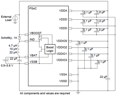
Figure 3.4: Application of Boost Converter Powering PSoC device
| Parameter | Description | Conditions | Min | Typ | Max | Units |
|---|---|---|---|---|---|---|
| LBOOST | Boost inductor | 4.7 μH nominal | 3.7 | 4.7 | 5.7 | μH |
| 10 μH nominal | 8.0 | 10.0 | 12.0 | μH | ||
| 22 μH nominal | 17.0 | 22.0 | 27.0 | μH | ||
| CBOOST | Total capacitance sum of VDDD, VDDA, VDDIO | 17.0 | 26.0 | 31.0 | μF | |
| CBAT | Battery filter capacitor | 17.0 | 22.0 | 27.0 | μF | |
| IF | Schottky diode average forward current | 1.0 | - | - | A | |
| VR | Schottky reverse voltage | 20.0 | - | - | V |
Boost Firmware Requirements:
- Disable Fast IMO During Startup:
- In PSoC Creator, open the design-wide resources (.cydwr) file.
- Navigate to the System tab.
- Locate the Enable Fast IMO During Startup option.
- Uncheck this option to ensure the device runs at 12 MHz during startup.
- Explanation:
- The PSoC device can optionally run at a faster clock speed (48 MHz) during startup for quicker configuration.
- However, this faster speed can lead to higher inrush current through the boost converter, potentially exceeding its specifications.
- By disabling the Fast IMO option, the device runs at a slower 12 MHz during startup, reducing the current draw and ensuring compliance with the boost converter's limits.
- Important Notes:
- This setting is crucial for designs utilizing the boost converter to prevent potential startup issues or damage to components.
- It's a simple configuration change within the PSoC Creator IDE that can significantly impact power management during the device's initial power-up phase.
Boost Design Process
Designing a PSoC Boost Converter requires a careful selection of component values based on unique operating conditions. This process involves determining the correct values for the CBAT capacitor, Inductor, Schottky diode, CBOOST capacitor, and specifically the inductor LBOOST.
Key Considerations:
- Operating Conditions: Carefully define the required input voltage (VBAT), output voltage (VOUT), ambient temperature (TA), and output current (IOUT) ranges for your application.
- Component Values: Most component values are fixed, but the inductor (LBOOST) value must be selected based on operating conditions and efficiency goals.
Operating Constraints: Ensure your desired operating conditions fall within the PSoC Boost Converter's allowable ranges for VOUT, VBAT, IOUT, and TA. - External Boost Regulator: If the PSoC Boost Converter cannot meet your specific requirements, consider using an external boost regulator instead.
Design Process:
- Define Operating Conditions:
- Specify the desired ranges for VBAT, VOUT, TA, and IOUT that align with your application's needs.
- Verify VBAT and VOUT Ranges:
- Consult Figure 3.5 to ensure your desired VBAT and VOUT ranges fall within the acceptable operating range of the PSoC Boost Converter.
- If not, either adjust your operating conditions or consider using an external boost regulator.
- Verify Ambient Temperature Range:
- Using Figure 3.5 again, confirm that your desired TA range is also within the converter's operating limits.
- If not, adjust operating conditions or consider an external regulator.
- Verify Output Current Range:
- Refer to Figure 3.6 to ensure your desired IOUT range is supported by the converter.
- If not, adjust operating conditions or consider an external regulator.
- Select Inductor Value:
- Use Figure 3.7 to determine the allowed inductor values based on your specific VBAT and VOUT requirements.
- Optimize Inductor Selection:
- Consider factors like inductor dimensions, cost, boost efficiency, and output voltage ripple (VRIPPLE) when choosing the final inductor value.
- Refer to Figures 3.8 through 3.11 for typical efficiency and VRIPPLE values.
- Generally, higher inductor values offer better efficiency and lower ripple, while smaller inductors may be preferred for cost or size constraints.
- If none of the allowed inductors meet your efficiency, ripple, cost, or size requirements, consider using an external boost regulator.
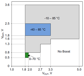
Figure 3.5: TA range over VBAT and VOUT
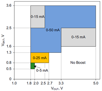
Figure 3.6: IOUT range over VBAT and VOUT
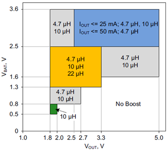
Figure 3.7: LBOOST range over VBAT and VOUT
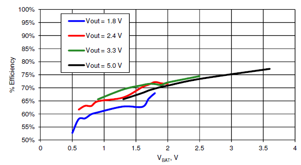
Figure 3.8: Efficiency vs VBAT, LBoost = 4.7 μH
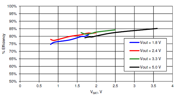
Figure 3.9: Efficiency vs VBAT, LBoost = 10 μH
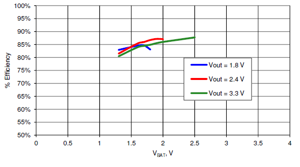
Figure 3.10: Efficiency vs VBAT, LBoost = 22 μH
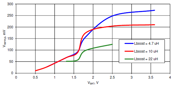
Figure 3.11: VRIPPLE vs VBAT
3.5 VDDIO Setting in PSoC Creator
Features and Benefits:
- Separate Analog and Digital Supplies: This design helps reduce cross-domain interference, which is crucial for applications requiring high precision and stability in analog readings.
- Dedicated Regulators for Different Domains: Each regulator is optimized for its respective domain, enhancing the efficiency and performance of the microcontroller.
- Support for Low-Power Modes: Including sleep and hibernate regulators facilitates efficient power management, making the PSoC 5LP suitable for battery-operated and energy-sensitive applications.
The power system architecture of the PSoC 5LP reflects a careful balance between performance, efficiency, and versatility, making it an ideal choice for a wide range of applications where power efficiency and reliable operation are critical.
Standard Power Configuration:
- No boost pump
- VDDA ≥ VDDD ≥ VDDIO0/1/2/3
- VDDA = 1.8 ~ 5.5V
Vdda must be the highest voltage present on the device. All other supply pins must be less than or equal to Vdda.
