Tiva Lab 11: Controlling a DC Motor and LED Using PWM
Objective
- Learn how to use the PWM signal to change the brightness of an LED and the speed of a small DC motor.
- Learn how to calculate the LOAD and CMP values for the PWM signal.
Required Reading Materials
- Lesson 13: Pulse-Width Modulation (PWM)
- Datasheet: LS293D
Overview
DC motor is a rotating machine that converts direct current electrical energy into mechanical energy. It is widely used in electrical power tools, toys, and appliances. They could be powered by a small battery to a DC power adapter. The basic working principle of a DC motor is that whenever a current-carrying conductor is placed in a magnetic field, it experiences a mechanical force that has the tendency to move. If the current direction is reversed, the motor's rotation will also reverse.
The speed control of DC motors for various applications is very important. There are two methods for controlling DC motor speed: current control and voltage control. Voltage control is not a good idea, as low voltage can cause torque loss; the best way to control speed is by current control. A simple way to control current is to add a variable resistor in series with the motor and adjust its resistance to change the current through the motor. But this method is not efficient, because the variable resistor also consumes energy.
The PWM (pulse width modulation) method is a very efficient method and is the most commonly used method. PWM uses digital signals to control the average power across analog devices. It is essentially a fixed-frequency square wave with adjustable pulse width. This method can achieve a smooth speed variation without reducing the motor's starting torque.
PWM Signals
The requirements of the PWM output signal in this lab are shown below:
- The frequency of the PWM output is 1000Hz
- The range of the duty cycle for PWM could be from 0% to 100%
- Right-aligned PWM signal
To calculate the PWM timer clock frequency, you have to know the default system clock frequency.
- EK-TM4C123GXL LaunchPad: You need to uncheck the "Clock Configuration" in the Keil μVision. After you uncheck the setting, the default system clock is 16 MHz
EK-TM4C123GXL LaunchPad
In Keil μVision, when you include the Startup pack in the project, the system clock frequency for the TM4C123G LaunchPad is configured to 50 MHz. The next step will help you to disable the clock configuration in Keil C.
- You can open the system_TM4C123.c (Startup) file, and click on the Configuration Wizard tab. Uncheck the Clock Configuration option to skip it.

- If the Clock Configuration is bypassed, the system clock will default to 16 MHz.
- You can open the system_TM4C123.c (Startup) file, and click on the Configuration Wizard tab. Uncheck the Clock Configuration option to skip it.
- EK-TM4C1294XL LaunchPad: By default, the system clock is 16 MHz.

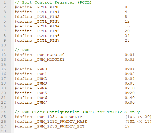
In this project, ezTivaLib will be imported, and its API will be used to configure the system clock frequency. Therefore, students must examine the template firmware source code to verify the exact system clock frequency used in the project.
Calculations
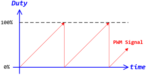
Figure 1: PWM Outputs for DC Motor and LED
You have to calculate the frequency of the PWM timer based on the system clock frequency and the PWM divisor.
${f_{PWMTimer}} = \frac{{SysClk}}{{PWMDivsor}}$
Calculate the count value for the PWM signal. This value will be set to the LOAD register, which is a 16-bit register only. If the count value you calculated is over 65535 (= 216-1), you need to reduce the frequency of the PWM Timer by increasing the value of the PWM Divisor and then recalculate the count value again.
$LOAD = Coun{t_{PWM}} = \frac{{{T_{PWM}}}}{{{T_{PWMTimer}}}} = \frac{{{f_{PWMTimer}}}}{{{f_{PWM}}}} \le 65535$
Changing the CMP value in the PWM module will change the duty cycle of the PWM signal. To calculate the CMP value, you have to know the type of PWM signal that you used: Left-aligned or right-aligned PWM.
- For Left-Aligned PWM:
- $duty = {t \over T} \times 100\% = 1 - {{CMP} \over {LOAD}}$
- If the CMP value is close to the LOAD value, it will decrease the duty cycle of the PWM signal.
- If the CMP value is closing to zero, it will increase the duty cycle of the PWM signal.
- For Right-Aligned PWM:
- $duty = {t \over T} \times 100\% = {{CMP} \over {LOAD}}$
- If the CMP value is close to the LOAD value, it will increase the duty cycle of the PWM signal.
- If the CMP value is close to zero, it will decrease the duty cycle of the PWM signal.
In this lab, the range of the duty cycle is from 0% to 100%, and the relationship between CMP and LOAD is:
$0 \le CMP < LOAD$
That means the value for the CMP register must be less than the LOAD value. The detailed calculations for CMP values can be found in this session.
Set the initial values of the duty cycle for both PWM outputs to 0%.
Components Required
| 5V DC Motor | × 1 | |
| 220ohm Resistor | × 3 | |
 |
L293D Motor Driver | × 1 |
 |
Breadboard | × 1 |
 |
Breadboard Power Module | × 1 |
| Power Adapter | × 1 |
Circuit Diagram
The motor will typically draw more current than a microcontroller can support. Therefore, the L293D will provide power to the motor, and its input pin connects to the PWM signal from the microcontroller. Plug the power supply module on the breadboard. The power supply module provides two power sources: +5V and +3.3V. Make sure the power source you connected to the circuit is +5V.
A breadboard power module must be used in this lab. Do not connect +5V from the Tiva board that directly connects to a USB port on the computer. Since the motor needs more current, it may cause USB overcurrent. If this happens, it will trigger a protection circuit to shut down the USB port. To reset the USB controller, disconnect the Tiva board from the USB port, shut the computer down (power off), and then power it on again.
In this lab, the microcontroller needs to generate two PWM signals. One is connected to a DC motor through a motor controller, and the other is connected to an onboard LED to control its brightness. The code needs to update the duty cycle on both PWM signals.
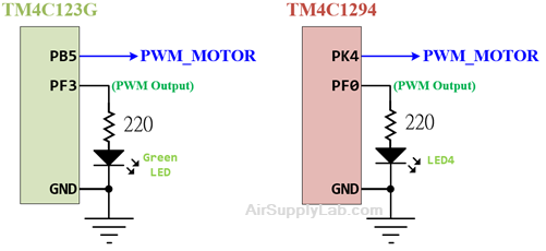
Port/Pin for TM4C123G
| Device | Port.Pin | Signal Type | PCTL | Direction | Drive Mode |
|---|---|---|---|---|---|
Port/Pin for TM4C1294
| Device | Port.Pin | Signal Type | PCTL | Direction | Drive Mode |
|---|---|---|---|---|---|
Procedure
- Create a new folder under the EE3450 folder and name it Lab10_PWMMotorLED.
- Launch the Keil μVisio and create a new project. Save the project to the folder you created in the previous step and set the project name to Lab10_PWMMotorLED.
- Add the Common and ezTivaLIB folder to the include paths, under the "Options for Target" setting.
- Add ezTiva LIB (ez123GLIB.lib or ez1294LIB.lib) into your project, and increase the stack and heap size under the "startup_TM4cXXX.s (Startup)" setting.
MyDefines.h
Add the following definitions to the MyDefines.h file:
Configurations
PWM Connection and Configuration
PWM Initialization & Configuration
Find the frequency of the system clock, and calculate the frequency of the PWM Timer.
| System Clock SysClk (Hz) |
PWMDIV | fPWMTimer = SysClk / PWMDIV (Hz) |
Check the PCTL table (for 123G or 1294) to find the pins which support PWM peripheral signal
| GPIO Port.Pin |
PWM Module |
PCTL | PWM | |||||||
| Module (m) |
Generator (n) |
Signal GEN | Output | Signal Type | Output Frequency fPWM |
LOAD Value (16-bit) |
Initial CMP Value (16-bit) |
|||
You have to know the frequency of the System Clock (1), the frequency of PWM output signal (2), and the initial value for duty cycle (3). Then, calculate the LOAD value and CMP value.
$LOA{D_{16bit}} = \frac{{{f_{PWMTimer}}}}{{{f_{PWM}}}}$
For Left-Aligned PWM Signals
Calculate CMP value by duty cycle (%):
$CM{P_{16bit}} = LOAD \times (1 - Dut{y_\% }) = \frac{{{f_{PWMTimer}}}}{{{f_{PWM}}}} \times (1 - Dut{y_\% })$
Calculate CMP value by pulse width:
$CM{P_{16bit}} = LOAD - \frac{{{T_{PulseWidth}}}}{{{T_{PWMTimer}}}} = ({T_{PWM}} - {T_{PulseWidth}}) \times {f_{PWMTimer}}$
For Right-Aligned PWM Signals
Calculate CMP value by duty cycle (%):
$CM{P_{16bit}} = LOAD \times Dut{y_\% } = \frac{{{f_{PWMTimer}}}}{{{f_{PWM}}}} \times Dut{y_\% }$
Calculate CMP value by pulse width:
$CM{P_{16bit}} = \frac{{{T_{PulseWidth}}}}{{{T_{PWMTimer}}}} = {T_{PulseWidth}} \times {f_{PWMTimer}}$
The following steps show how to initialize PWM peripheral.
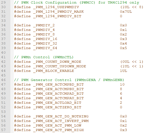
- Enable Clock to the PWM Modules (RCGCPWM register)
TM4C123G:
SYSCTL->RCGCPWM = MyDefines.h8 4 2 1 8 4 2 1 7 6 5 4 3 2 1 0 bit PWM
Module 1PWM
Module 0PWM 0 0 0 0 - 0 0
= binary = hex
TM4C1294:
SYSCTL->RCGCPWM = MyDefines.h8 4 2 1 8 4 2 1 7 6 5 4 3 2 1 0 bit PWM
Module 0PWM 0 0 0 0 - 0 0 0
= binary = hex
After enable clock signal, check the PRPWM register until the corresponding bit set to 1.
In C:
while ( (SYSCTL->PRPWM & (__) ) != (____ )) {}; - Enable and Setup Clock Divider for all PWM modules
USEPWMDIV: Enable PWM Clock Divisor
- 0: The system clock is the source for the PWM clock
- 1: The PWM clock divider is the source for the PWM clock
PWMDIV: PWM Unit Cloxk Divisor
- 0x0: /2
- 0x1: /4
- 0x2: /8
- 0x3: /16
- 0x4: /32
- 0x5: /64
TM4C123G:
SYSCTL->RCC &= ~(0x7 << 17); // RCC[19:17]=000 PWMDIVRCC 31 ~ 21 20 19 ~ 17 16 ~ 0 bit USEPWMDIV PWMDIV x x
SYSCTL->RCC |=
|= |=
TM4C1294:
PWM0->CC &= ~(0x7); // PWMCC[2:0]=000 PWMDIVPWMCC 31 ~ 9 8 7 ~ 3 2 ~ 0 bit USEPWMDIV PWMDIV x x
PWM0->CC |=
|= |= - PWM Signal Generation Control Register (PWMnCTL)
MODE: Counter Mode
- 0: Count-Down mode
- 1: Count-Up/Down mode
ENABLE: PWM Block Enable
- 0: The entire PWM generation block is disable and not not clocked
- 1: The PWM generation block is enabled and produces PWM signals
PWMnCTL 31 ~ 19 18 17 16 15 ~ 14 13 ~ 12 11 ~ 10 9 ~ 8 bit LATCH MINFLTPER FLTSRC DBFALLUPD DBRISEUPD DBCTLUPD GENBUPD x PWMnCTL 7 ~ 6 5 4 3 2 1 0 bit GENAUPD CMPBUPD CMPAUPD LOADUPD DEBUG MODE ENABLE PWM ->_ _CTL =
= = - Setup the Period of the PWM Signal (PWMnLOAD)
The 16-bit LOAD value is used to control the PWM period.
PWMnLOAD 31 ~ 16 15 ~ 0 bit LOAD PWM ->_ _LOAD =
- Setup the Initial Duty Cycle (PWMnCMPA / PWMnCMPB)
The PWMnCMPA / PWMnCMPB registers are used to compare against the PWM counter. When this value matches the counter, a pulse is output which can be configured to drive the pwmA and pwmB signals (via the PWMnGENA and PWMnGENB).
PWMnCMPA 31 ~ 16 15 ~ 0 bit CMPA PWM ->_ _CMPA =
PWMnCMPB 31 ~ 16 15 ~ 0 bit CMPB PWM ->_ _CMPB =
- Setup PWM Signal Type (PWMnGENA / PWMnGENB)
These register control the generation of the pwmA/pwmB signal based on the load and zero output pulses from the counter, as well as the compare A (CMPA) and compare B (CMPB) pulses from the comparators.
- 0x0: Do nothing
- 0x1: Invert PWM signal
- 0x2: Drive PWM signal Low
- 0x3: Drive PWM signal High
ACTCMPBD: Action for Comparator B in count-down mode
ACTCMPBU: Action for Comparator B in count-up mode
ACTCMPAD: Action for Comparator A in count-down mode
ACTCMPAU: Action for Comparator A in count-up mode
ACTLOAD: Action for Counter = LOAD
ACTZERO: Action for Counter = 0
Counter running in Count-Down mode
PWMnGENA/B 31 ~ 12 11 ~ 10 9 ~ 8 7 ~ 6 5 ~ 4 3 ~ 2 0 ~ 1 bit ACTCMPBD ACTCMPBU ACTCMPAD ACTCMPAU ACTLOAD ATZERO x PWM ->_ _GENA =
= =PWM ->_ _GENB =
= =
Counter running in Count-Up/Down mode
PWMnGENA/B 31 ~ 12 11 ~ 10 9 ~ 8 7 ~ 6 5 ~ 4 3 ~ 2 0 ~ 1 bit ACTCMPBD ACTCMPBU ACTCMPAD ACTCMPAU ACTLOAD ATZERO PWM ->_ _GENA =
= =PWM ->_ _GENB =
= = - PWM Output Enable (PWMnENABLE)
This register provides a master control of which PWM signals are output to the GPIO pins. By disabling a PWM output, the PWM generation process can continue without driving PWM signals to the pins.
- 0: The PWM signal has a zero value
- 1: The generated PWM signal is passed to the GPIO pin
8 4 2 1 8 4 2 1 7 6 5 4 3 2 1 0 bit PWM Module PWM
7PWM
6PWM
5PWM
4- PWM
3PWM
2PWM
1PWM
0pin Value in Hex Register Value to Register - - = ➤ PWM ->ENABLE - - = ➤ PWM ->ENABLE
GPIO Initialization and Configuration
GPIO Initialization Configuration
Next, we need to configure all the GPIO ports and pins that are used in the design.
According to the pin connections, complete the following GPIO configurations for each port. Fills the pin field by the value below:
- 0: Clean the bit
- 1: Set the bit
- x: Do not change the bit
- d: Do not care
For both TM4C123GXL and TM4C1294XL LaunchPads, the Port C [3:0] are used for JTAG/SWD. Therefore, when you configure Port C, you have to use bitwise operators to make sure your new configuration settings do not affect the JTAG/SWD function (PC3 ~ PC0).
Most of GPIO pins are configured as GPIOs and tri-stated by default (GPIOPCTL = 0, CPIOAFSEL = 0, GPIODIR = 0, GPIOPUR = 0, GPIOPDR = 0, GPIOODR = 0)
- Enable Clock to the GPIO Modules (RCGCGPIO register)
TM4C123G: SYSCTL->RCGCGPIO |= (_PORTs); |= binary = hex
8 4 2 1 8 4 2 1 7 6 5 4 3 2 1 0 bit Port F Port E Port D Port C Port B Port A port 0 0 -
TM4C1294: SYSCTL->RCGCGPIO |= (_PORTs); |= binary = hex
After enabling the clock signal, check the PRGPIO register until the corresponding bit is set to 1.8 4 2 1 8 4 2 1 8 4 2 1 8 4 2 1 15 14 13 12 11 10 9 8 7 6 5 4 3 2 1 0 bit Port Q Port P Port N Port M Port L Port K Port J Port H Port G Port F Port E Port D Port C Port B Port A port 0 - - -
In Assembly:
            LDR     R0, =SYSCTL_PRGPIO_R
Wait4GPIO   LDR     R1, [R0]
            TST     R1, #(__)
            BEQ     Wait4GPIO
In c:
while ( (SYSCTL->PRGPIO & ____ ) != ____ ) {}; - Unlock Port
TM4C123G: PD7 and PF0 are locked after reset.
TM4C1294: PD7 and PE7 are locked after reset
If those pins are used in the design, they must be unlocked first. To unlock the port, 0x4C4F434B must be written into the GPIOLOCK register and uncommit it by setting the GPIOCR register.
8 4 2 1 8 4 2 1 7 6 5 4 3 2 1 0 bit Port Pin 7 Pin 6 Pin 5 Pin 4 - Pin 3 Pin 2 Pin 1 Pin 0 pin Value in Hex Register Value to Register - - = ➤ GPIO ->LOCK = 0x4C4F434B - - = ➤ GPIO ->CR - - = ➤ GPIO ->LOCK = 0x4C4F434B - - = ➤ GPIO ->CR
Convert above configuration into registers
- GPIO Analog Mode Select
If any pin is used as an Analog signal (check Signal Type field on table 1), the appropriate bit in AMSEL must be set.
- 0: Digital signal
- 1: Analog signal
8 4 2 1 8 4 2 1 7 6 5 4 3 2 1 0 bit Port Pin 7 Pin 6 Pin 5 Pin 4 - Pin 3 Pin 2 Pin 1 Pin 0 pin Value in Hex Register Value to Register - - = ➤ GPIO ->AMSEL - - = ➤ GPIO ->AMSEL - - = ➤ GPIO ->AMSEL - - = ➤ GPIO ->AMSEL - - = ➤ GPIO ->AMSEL - - = ➤ GPIO ->AMSEL - - = ➤ GPIO ->AMSEL - GPIO Port Control (PCTL)
The PCTL register is used to select the specific peripheral signal for each GPIO pin when using the alternate function mode.
- 0: GPIO
- 1~0xF: Check the GPIO Pins and Alternate Function table
8421 8421 8421 8421 8421 8421 8421 8421 31~28 27~24 23~20 19~16 15~12 11~8 7~4 3~0 bit Port Pin 7 Pin 6 Pin 5 Pin 4 - Pin 3 Pin 2 Pin 1 Pin 0 pin Value in Hex Register Value to Register - - = ➤ GPIO ->PCTL - - = ➤ GPIO ->PCTL - - = ➤ GPIO ->PCTL - - = ➤ GPIO ->PCTL - - = ➤ GPIO ->PCTL - - = ➤ GPIO ->PCTL - - = ➤ GPIO ->PCTL - GPIO Alternate Function Select (AFSEL)
Setting a bit in the AFSEL register configures the corresponding GPIO pin to be controlled by PCTL peripheral function.
- 0: General I/O
- 1: Pin connected to the digital function defined in the PCTL register
8 4 2 1 8 4 2 1 7 6 5 4 3 2 1 0 bit Port Pin 7 Pin 6 Pin 5 Pin 4 - Pin 3 Pin 2 Pin 1 Pin 0 pin Value in Hex Register Value to Register - - = ➤ GPIO ->AFSEL - - = ➤ GPIO ->AFSEL - - = ➤ GPIO ->AFSEL - - = ➤ GPIO ->AFSEL - - = ➤ GPIO ->AFSEL - - = ➤ GPIO ->AFSEL - - = ➤ GPIO ->AFSEL - GPIO Pin Direction (DIR)
Set pin direction
- 0: Input pin
- 1: Output pin
8 4 2 1 8 4 2 1 7 6 5 4 3 2 1 0 bit Port Pin 7 Pin 6 Pin 5 Pin 4 - Pin 3 Pin 2 Pin 1 Pin 0 pin Value in Hex Register Value to Register - - = ➤ GPIO ->DIR - - = ➤ GPIO ->DIR - - = ➤ GPIO ->DIR - - = ➤ GPIO ->DIR - - = ➤ GPIO ->DIR - - = ➤ GPIO ->DIR - - = ➤ GPIO ->DIR - Internal Pull-Up Resistor (PUR), Pull-Down Resistor (PDR), and Open-Drain (ODR)
PUR: The pull-up control register
PDR: The pull-down control register
ODR: The open-drain control register
- 0: Disable
- 1: Enable
8 4 2 1 8 4 2 1 7 6 5 4 3 2 1 0 bit Port Pin 7 Pin 6 Pin 5 Pin 4 - Pin 3 Pin 2 Pin 1 Pin 0 pin Value in Hex Register Value to Register - - = ➤ GPIO -> - - = ➤ GPIO -> - - = ➤ GPIO -> - - = ➤ GPIO -> - - = ➤ GPIO -> - - = ➤ GPIO -> - - = ➤ GPIO -> - GPIO Digital Enable
Enables all the pins that are used in the design, including GPIO pins and alternate function pins.
- 0: Pin undriven
- 1: Enable pin
8 4 2 1 8 4 2 1 7 6 5 4 3 2 1 0 bit Port Pin 7 Pin 6 Pin 5 Pin 4 - Pin 3 Pin 2 Pin 1 Pin 0 pin Value in Hex Register Value to Register - - = ➤ GPIO ->DEN - - = ➤ GPIO ->DEN - - = ➤ GPIO ->DEN - - = ➤ GPIO ->DEN - - = ➤ GPIO ->DEN - - = ➤ GPIO ->DEN - - = ➤ GPIO ->DEN
Sample Firmware Code
EK-TM4C123GXL LaunchPad
The PB5 and PF3 are configured as PWM signal output. Both have the same configuration and the same CMP value.
Keil C Sample Firmware Code
#include <stdio.h>
#include <stdlib.h>
#include <stdint.h>
#include <stdbool.h>

#include "TM4C123GH6PM.h"
#include "MyDefines.h"  // Your Definitions Header File
#include "ez123G.h"

void Setup_PWM(void);
void Setup_GPIO(void);

int main()
{
    uint16_t    cmpDuty[]={ ....};

    Setup_123G_80MHz();    // Configure System Clock to 80 MHz
	Setup_PWM();
    Setup_GPIO();

    while(1){
        // Place your application code here

    }
}
//------------------------------------------------------------------------------
// SysClk = ? Hz, PWMDIV = /?, Freq for PWMTimer = ? Hz
// GPIO for PWM: Pxx
    // M?PWM? - PWM Module(m) ?, generator(g) ?, GENA/B, PWM?, PCTL = ?
    // PWM frequency = ? Hz
    // LOAD = ?
    // CMP  = ?
// GPIO for PWM: Pxx
    // M?PWM? - PWM Module ?, generator ?, GENA/B, PWM?, PCTL = ?
    // PWM frequency = ? Hz
    // LOAD = ?
    // CMP  = ?
void Setup_PWM(void)
{
    // 1. Enable Clock for PWM Modules
    SYSCTL->RCGCPWM |= (__);
    while((SYSCTL->PRPWM & (__)) != (__)){};
    // 2. Enable and Setup Clock Divider for PWM Timer
    SYSCTL->RCC |= (_PWM_123G_USEPWMDIV);                   // RCC[20]=1:USEPWMDIV
    SYSCTL->RCC &= ~(_PWM_123G_PWMDIV_MASK);                // RCC[19:17]=000 PWMDIV
    SYSCTL->RCC |= (_PWMDIV_? << _PWM123G_PWMDIV_BIT );     // RCC[19:17]=divisor
    // 3. Disable PWM Blocks and Setup the Timer Counting Mode
    PWMm->_g_CTL = 0x00;                            // Disable PWM Generator, and set to count-down mode
    PWMm->_g_CTL = 0x00;                            // Disable PWM Generator, and set to count-down mode
    // 4. Configure LOAD, CMP, and GEN values
    PWMm->_g_LOAD = ____;
    PWMm->_g_CMPx = ____;
    PWMm->_g_GENx = (_PWM_GEN_ACT_PWM_HIGH << ____) |
                    (_PWM_GEN_ACT_PWM_LOW  << ____);    // Right-Aligned PWM

    PWMm->_g_LOAD = ____;
    PWMm->_g_CMPx = ____;
    PWMm->_g_GENx = (_PWM_GEN_ACT_PWM_HIGH << ____) |
                    (_PWM_GEN_ACT_PWM_LOW  << ____);    // Right-Aligned PWM
    // 5. Enable PWM Blocks
    PWMm->_g_CTL |= ____;
    PWMm->_g_CTL |= ____;
    // 6. Enable PWM outputs on each PWM module
    PWMm->ENABLE  = ____;
    PWMm->ENABLE  = ____;
}
//------------------------------------------------------------------------------
/*
Device      Port.Pins       DIR     DriveMode
PWM_MOTOR
LED

Port ____
*/

void Setup_GPIO(void)
{
    // GPIO Initialization and Configuration
    // 1. Enable Clock to the GPIO Modules (SYSCTL->RCGCGPIO |= (_PORTs);)
    SYSCTL->RCGCGPIO |= (__);
    // allow time for clock to stabilize (SYSCTL->PRGPIO & (_PORTs))
    while((SYSCTL->PRGPIO & (__)) != (__)){};
    // 2. Unlock GPIO only PD7, PF0 on TM4C123G; PD7 on TM4C1294 (GPIOx->LOCK = 0x4C4F434B; and GPIOx->CR = _PINs;)
    // 3. Set Analog Mode Select bits for each Port (GPIOx->AMSEL = _PINs;  0=digital, 1=analog)
    // 4. Set Port Control Register for each Port (GPIOx->PCTL = PMCn << _PTCL_PINn, check the PCTL table)

    // 5. Set Alternate Function Select bits for each Port (GPIOx->AFSEL = _PINs;  0=regular I/O, 1=PCTL peripheral)

    // 6. Set Output pins for each Port (Direction of the Pins: GPIOx->DIR = _PINs;  0=input, 1=output)
    // 7. Set PUR bits (internal Pull-Up Resistor), PDR (Pull-Down Resistor), ODR (Open Drain) for each Port
    // 8. Set Digital ENable register on all port.pins (GPIOx->DEN = _PINs;)

}
EK-TM4C1294XL LaunchPad
The PF0 and PK4 are configured as PWM signal output. Both have the same configuration and the same CMP value.
Keil C Sample Firmware Code
#include <stdio.h>
#include <stdlib.h>
#include <stdint.h>
#include <stdbool.h>

#include "TM4C1294NCPDT.h"
#include "MyDefines.h"  // Your Definitions Header File
#include "ez1294.h"

void Setup_PWM(void);
void Setup_GPIO(void);

int main()
{
    uint16_t    cmpDuty[]={ ....};

    Setup_1294_96MHz();    // Configure System Clock to 96 MHz
	Setup_PWM();
    Setup_GPIO();

    while(1){
        // Place your application code here

    }
}
//------------------------------------------------------------------------------
// SysClk = ? Hz, PWMDIV = /?, Freq for PWMTimer = ? Hz
// GPIO for PWM: Pxx
    // M?PWM? - PWM Module ?, generator ?, GENA/B, PWM? , PCTL = ?
    // PWM frequency = ? Hz
    // LOAD = ?
    // CMP  = ?
// GPIO for PWM: Pxx
    // M?PWM? - PWM Module ?, generator ?, GENA/B, PWM?
    // PWM frequency = ? Hz
    // LOAD = ?
    // CMP  = ?

void Setup_PWM(void)
{
    // 1. Enable Clock for PWM Module
    SYSCTL->RCGCPWM |= (__);
    while((SYSCTL->PRPWM & (__)) != (__)){};
    // 2. Enable and Setup Clock Divider for PWM Timer
    PWMm->CC |= (_PWM_1294_USEPWMDIV);                          // CC[8]:USEPWMDIV
    PWMm->CC &= ~(_PWM_1294_PWMDIV_MASK);                       // CC[2:0]=000 PWMDIV
    PWMm->CC |= (_PWMDIV_? << _PWM_1294_PWMDIV_BIT);			// CC[2:0]=divisor
    // 3. Disable PWM Blocks and Setup the Timer counting mode
    PWMm->_g_CTL = 0x00;                            // Disable PWM Generator, and set to count down mode
    PWMm->_g_CTL = 0x00;                            // Disable PWM Generator, and set to count down mode
    // 4. Configure LOAD, CMP, and GEN values
    PWMm->_g_LOAD = ____;
    PWMm->_g_CMP? = ____;
    PWMm->_g_GEN? = (_PWM_GEN_ACT_PWM_HIGH << ____) |
                    (_PWM_GEN_ACT_PWM_LOW  << ____);    // Right-Aligned PWM

    PWMm->_g_LOAD = ____;
    PWMm->_g_CMP? = ____;
    PWMm->_g_GEN? = (_PWM_GEN_ACT_PWM_HIGH << ____) |
                    (_PWM_GEN_ACT_PWM_LO W << ____);    // Right-Aligned PWM
    // 5. Enable PWM Blocks
    PWMm->_g_CTL |= ____;
    PWMm->_g_CTL |= ____;
    // 6. Enable PWM outputs on each PWM module
    PWMm->ENABLE  = ____;
    PWMm->ENABLE  = ____;
}
//------------------------------------------------------------------------------
/*
Device      Port.Pins       DIR     DriveMode
PWM_MOTOR
LED

Port ____
*/

void Setup_GPIO(void)
{
    // GPIO Initialization and Configuration
    // 1. Enable Clock to the GPIO Modules (SYSCTL->RCGCGPIO |= (_PORTs);)
    SYSCTL->RCGCGPIO |= (__);
    // allow time for clock to stabilize (SYSCTL->PRGPIO & (_PORTs))
    while((SYSCTL->PRGPIO & (__)) != (__)){};
    // 2. Unlock GPIO only PD7, PF0 on TM4C123G; PD7 on TM4C1294 (GPIOx->LOCK = 0x4C4F434B; and GPIOx->CR = _PINs;)
    // 3. Set Analog Mode Select bits for each Port (GPIOx->AMSEL = _PINs;  0=digital, 1=analog)
    // 4. Set Port Control Register for each Port (GPIOx->PCTL = PMCn << _PTCL_PINn, check the PCTL table)

    // 5. Set Alternate Function Select bits for each Port (GPIOx->AFSEL = _PINs;  0=regular I/O, 1=PCTL peripheral)

    // 6. Set Output pins for each Port (Direction of the Pins: GPIOx->DIR = _PINs;  0=input, 1=output)
    // 7. Set PUR bits (internal Pull-Up Resistor), PDR (Pull-Down Resistor), ODR (Open Drain) for each Port
    // 8. Set Digital ENable register on all port.pins (GPIOx->DEN = _PINs;)

}
Lab Experiments
Experiment Procedure:
In this experiment, you will generate several PWM duty cycle levels and switch between them every 2 seconds.
Step 1: Calculate the CMP Values
Manually calculate the 'CMP' values for the following duty cycles:
- 0%
- 40%
- 70%
- 100%
After calculating the values, store them in an integer array named 'cmpDuty[]'.
Step 2: Create the Required Variables
Create the following variables in your program:
- An integer array 'cmpDuty[]' with the initial 'CMP' values
- An integer variable 'i', initialized to '0'
Step 3: Update the PWM Duty Cycle Repeatedly
Inside the main loop, perform the following steps repeatedly:
- Set both PWMm->_g_CMP? registers to the value stored in cmpDuty[i].
- Increase i by 1.
- If i is greater than the array's maximum valid index, reset i to 0.
- Delay for 2000 ms before changing to the next duty cycle.
You have to use a delay function provided by ezTivaLIB.
Step 4: Repeat Forever
Continue looping so the PWM output cycles through all duty cycle settings continuously.
Pseudocode:
REPEAT:
    Set both PWMm->_g_CMP? to cmpDuty[i]
    i = i + 1
    If i > max index of cmpDuty[]
        i = 0
    Delay 2000 ms
LOOP
Exp #7.1: Positive/Negative Logic Output for Motor Driver
Part 1
In the first experiment, connect the DC motor to the L293D controller by using positive logic output as shown in the following diagram.
- Disconnect the power.
- Connect the red wire on the motor to the L293D output pin (pin 14) and the black wire to the ground pin.
- Turn on the power. Observe the motor speed changing during the duty cycle changes and record the results in Question 2.
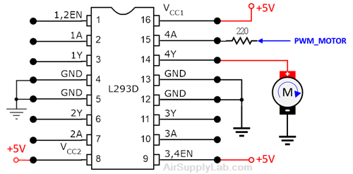
Figure 2: The Connection of Positive Logic Output to Motor
Part 2
In the second experiment, change the motor connection to negative logic output as shown as follows, and then compare the result with positive logic output. (The motor rotation direction should be the same as Lab 1.)
- Turn off the power.
- Rewire the motor connections: the red wire on the motor to +5 V power and the black wire to the L293D output pin (pin 14).
- Turn on the power. Observe the motor speed changing and record the results in Question 2.
- Compare the result with the first part, and write down your observation about the maximum (highest) speed difference between the positive and negative logic outputs in your lab report.
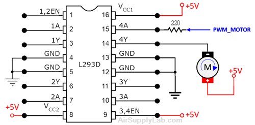
Figure 3: The Connection of Negative Logic Output to Motor
Questions
- What is the truth table for the L293D chip? (Read the L293D datasheet)
- Observes the motor speed in experiments 1 and 2, what is the difference after changing the wire connection on the motor? Explain why?
Exp Duty Cycle 0% 40% 70% 100% Part 1: Motor Speed (Hi+/Hi/Med/Lo/0) Part 2: Motor Speed (Hi+/Hi/Med/Lo/0) - How to produce a right-aligned PWM signal when you configure the GEN register? Explain it.
- If the System Clock is 50 MHz, and the frequency of the PWM outputs is 200 Hz. Calculate the following values:
- PWM Divisor value:
- LOAD value:
- CMP value for 25% duty cycle in Left-Aligned PWM signal:
- CMP value for 10% duty cycle in Right-Aligned PWM signal:
- What happens if the CMP value is set as the LOAD value? (In your code, set the CMP value to the same as the LOAD value, and observe the motor speed)
Exp #7.2: Change Motor Direction and Speed
You have already learned how to control motor speed using the PWM signal. Now, you must redesign the system to control the direction of motor rotation.
- Add two switches, SW1 and SW2, to the project onboard.
- SW1 is used to change the motor speed - whenever the user presses the SW1, the duty cycle will be changed to the next level from 0%, 40%, 70% to 100%, and then back to 0%.
- SW2 is used to change the motor direction - when the user presses the SW2, the motor rotation direction changes. (Do not change the rotation direction if the motor's duty cycle is not 0%)
- All actions are triggered when the switches are on the falling edge.
- Add two GPIO output pins, DIRA and DIRB, to change the output current direction through the motor to change the rotation direction.
- The frequency of the PWM output signals is 400 Hz.
Port/Pin for TM4C123G
| Device | Port.Pin | Signal Type | PCTL | Direction | Drive Mode |
|---|---|---|---|---|---|
Port/Pin for TM4C1294
| Device | Port.Pin | Signal Type | PCTL | Direction | Drive Mode |
|---|---|---|---|---|---|
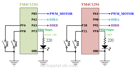
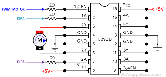
The current through the motor must be reversed to reverse the motor rotation direction. Connect the motor to the 1Y and 2Y output pins of L293D; connect the DIRA and DIRB to 1A and 2A input ping with 220-ohm resistors, and connect PWM_MOTOR signal to the 1,2EN pin through a 220-ohm resistor.
Inside the L293D chip, the DIRA and DIRB are connected to two buffer gates controlled by the 1,2EN pin. The outputs of the buffer gates control the motor's current direction. The bidirectional DC motor control circuit and truth table are given below:
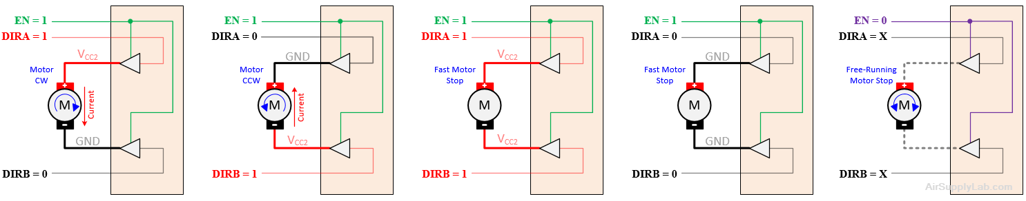
| Enable | DIRB | DIRA | Function |
|---|---|---|---|
| 0 | X | X | Free-Running, Motor Stop |
| 1 | 0 | 0 | Fast Motor Stop |
| 1 | 0 | 1 | Motor Turn CW |
| 1 | 1 | 0 | Motor Turn CCW |
| 1 | 1 | 1 | Fast Motor Stop |
In the main() function, after initializing the PWM and GIOP modules, you must set DIRA and DIRB values before the infinite loop so Moto can spin according to the duty cycles.
The procedure for changing the motor direction is listed below:
- If the current duty cycle is 0% (motor stops), then skip this procedure.
- Stop the motor: Set the duty cycle to 0% for 2 seconds to allow enough time for the motor to stop spinning.
- Change the motor rotation direction: Set the proper output values of DIRA and DIRB to change the direction of the current through the motor.
- Restore the PWM duty cycle value: The motor continues to rotate in the opposite direction.