FPGA Lab 02: Comparator, Decoders, and Encoders
Objective
Required Reading Materialss
Overview
Digital Comparators
Digital Comparators
A digital comparator is a combinational circuit that compares two binary values and determines their relative magnitudes. It is a crucial component in digital systems, used for tasks such as data sorting, error detection, and decision-making processes.
Functions of a Digital Comparator:
A digital comparator typically has three main outputs:
- A > B: Indicates that the first number (A) is greater than the second number (B).
- A = B: Indicates that the first number (A) is equal to the second number (B).
- A < B: Indicates that the first number (A) is less than the second number (B).
Implementation of a Digital Comparator:
Digital comparators can be implemented using various logic gates. The basic idea is to compare the bits of the numbers, starting from the most significant bit (MSB) to the least significant bit (LSB).
For example, a 1-bit comparator can be implemented using basic logic gates:
Table 2.1: Truth Table of the One-Bit Comparator
| Inputs | Output | |||
|---|---|---|---|---|
| A | B | A > B gt |
A = B eq |
A < B lt |
| 0 | 0 | 0 | 1 | 0 |
| 0 | 1 | 0 | 0 | 1 |
| 1 | 0 | 1 | 0 | 0 |
| 1 | 1 | 0 | 1 | 0 |
Based on Table 2.1, we can obtain logic functions between inputs and outputs of the one-bit comparator as follows:
- Equality (A = B): $\overline {A \oplus B} = A \odot B$
- Greater than (A > B): $A \cdot \overline B $
- Less than (A < B): $\overline A \cdot B$
The implementation can be cascaded from multiple single-bit comparators or designed using more complex combinational logic for multi-bit comparators.
Lab Experiments
2.1 Design a 4-bit Comparator
Objective:
Design a 4-bit comparator by creating a 2-bit comparator and then combining them.
Step 1: Design a 2-bit Comparator
Step 1: Design a 2-bit Comparator
- Truth Table Creation:
- Create a truth table for the 2-bit comparator with inputs
- Outputs are GT (Greater Then), EQ (Equal), and LT (Loess Then).
- Karnaugh Maps (K-Maps):
- Based on the truth table, draw K-maps for each output (GT, EQ, LT).
- Simplify the Boolean expressions using K-map techniques.
- Boolean Expressions:
- Derive simplified Boolean expressions for GT, EQ, and LT from the K-maps.
- Verilog Code for 2-bit Comparator:
- Implement the Boolean expressions in Verilog.
| Inputs | Output | |||||
|---|---|---|---|---|---|---|
| A1 | A0 | B1 | B0 | A > B GT |
A = B EQ |
A < B LT |
| 0 | 0 | 0 | 0 | |||
| 0 | 0 | 0 | 1 | |||
| 0 | 0 | 1 | 0 | |||
| 0 | 0 | 1 | 1 | |||
| 0 | 1 | 0 | 0 | |||
| 0 | 1 | 0 | 1 | |||
| 0 | 1 | 1 | 0 | |||
| 0 | 1 | 1 | 1 | |||
| 1 | 0 | 0 | 0 | |||
| 1 | 0 | 0 | 1 | |||
| 1 | 0 | 1 | 0 | |||
| 1 | 0 | 1 | 1 | |||
| 1 | 1 | 0 | 0 | |||
| 1 | 1 | 0 | 1 | |||
| 1 | 1 | 1 | 0 | |||
| 1 | 1 | 1 | 1 | |||
| GT | {B1, B0} | ||||
| 00 | 01 | 11 | 10 | ||
| {A1, A0} | 0 0 | 0 | 1 | 3 | 2 |
| 0 1 | 4 | 5 | 7 | 6 | |
| 1 1 | 12 | 13 | 15 | 14 | |
| 1 0 | 8 | 9 | 11 | 10 |
GT =
| EQ | {B1, B0} | ||||
| 00 | 01 | 11 | 10 | ||
| {A1, A0} | 0 0 | 0 | 1 | 3 | 2 |
| 0 1 | 4 | 5 | 7 | 6 | |
| 1 1 | 12 | 13 | 15 | 14 | |
| 1 0 | 8 | 9 | 11 | 10 |
EQ =
| LT | {B1, B0} | ||||
| 00 | 01 | 11 | 10 | ||
| {A1, A0} | 0 0 | 0 | 1 | 3 | 2 |
| 0 1 | 4 | 5 | 7 | 6 | |
| 1 1 | 12 | 13 | 15 | 14 | |
| 1 0 | 8 | 9 | 11 | 10 |
LT =
- Draw the logic circuits for the two-bit comparator with outputs GT, EQ, and LT.
- Implement the two-bit comparator using Gate-Level modeling in Verilog.
module comparator_2bit (a1, a0, b1, b0, gt, eq, lt);
input  a1, a0, b1, b0;
output gt, eq, lt;


// Your code here


endmodule
...
Step 2: Connect two 2-bit comparators to build a 4-bit comparator
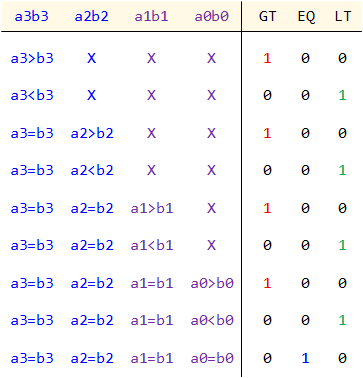
- A 4-bit comparator will use 4-bit input A and 4-bit input B. Therefore, the function table of the 4-bit comparator is shown below.

- Since the 4-bit comparator is built by using two 2-bit comparators to compare higher 2-bit of input A and B and lower 2-bit of A and B, the function table based on the previous 4-bit function table can be built as below:
G1 E1 L1 G0 E0 L0 GT EQ LT
GT =
EQ =
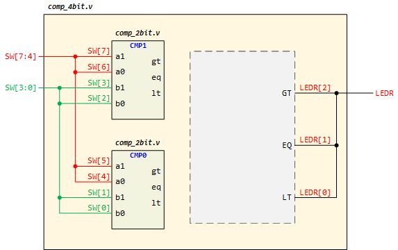
LT = - Complete the cmp_4bit.v module as the following block diagram.

- Compile the code and check the RTL Viewer. If there are no errors, program and test the code to the FPGA board.
- Use the following table to test your system.
A
SW[7:4]B
SW[3:0]GT
LEDR[2]EQ
LEDR[1]LT
LEDR[0]