FPGA Lab 03: Numbers and Displays
Reading Materials
Lab Experiments
3.1 Display Decimal
Objective
Design a circuit to convert a 4-bit binary number (B[3:0]) into a two-digit decimal equivalent (D = d1d0).
Information
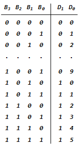
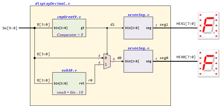
You are tasked with designing a circuit that converts a 4-bit binary number B[3:0] into its two-digit decimal equivalent D = d1d0. Table 1 shows the required output values. A partial design of this circuit is given in Figure 1. It includes a comparator that checks when the value of B is greater than 9 and uses the output of this comparator in the control of the 7-segment displays. Your task is to complete the design of this circuit.
Table 1: Binary-to-Decimal Conversion Values
The output gt signal for the comparator circuit can be specified using a single wire, with the four inputs B[3:0]. Design this Boolean expression by making a truth table that shows the valuations of the inputs B[3:0] for which gt has to be 1.

Figure 1: The Design of Binary-to-Decimal Conversion Circuit
Notice that the circuit in Figure 1 includes a 4-bit wide 2-to-1 multiplexer (a similar multiplexer was described as part of Lab 1.2). The purpose of this multiplexer is to drive digit d0 with the value of B when d1 = 0, and the value of r0 when d1 = 1.
To design the sub10 circuit, consider the following:
- For the input value B≤ 9, the circuit sub10 does not matter because the multiplexer in Figure 1 selects B in these cases.
- But, for the input values B > 9, the multiplexer will select r0 (the output of the sub10 module).
Thus, sub10 has to provide output values that properly implement Table 1 when the output result = 0001, …, and the input B = 1111 gives the output result = 0101. Design the sub10 circuit by making a truth table with the inputs bin[3:0] and the output result[3:0].
Step-by-Step Instructions
Perform the following steps:
- Launch Altera Quartus Prime and create a new project:
- Project working directory: <your project home folder>\Lab03.1_DisplayDecimal
- Project name: displayDecimal
- Top-level module name: displayDecimal
- Create a new Verilog HDL file:
- Implement the top module to Integrate the comparator, multiplexer, subtraction, and seven-segment display modules
- Save it to the displayDecimal.v file.
module displayDecimal(SW, HEX0, HEX1); input [9:0] SW; output [7:0] HEX0; output [7:0] HEX1; wire d1; wire [3:0] d0; wire [3:0] r0; wire [7:0] seg0; wire [7:0] seg1; wire [3:0] B; assign B = SW[3:0]; assign HEX0 = seg0; assign HEX1 = seg1; cmpGreat9 U1 (.bin( ), .gt( )); sub10 U2 (.bin( ), .ret( )); mux2to1_4bit U3 (.in0( ), .in1(), .sel( ), .out( )); sevenSeg U4 (.bin( ), .seg( )); sevenSeg U5 (.bin( ), .seg( )); endmodule - Create the comparator module:
- Implement the comparator module that determines if the 4-bit binary number is greater than 9 or not.
- Save it to the cmpGreat9.v file.
module cmpGreat9(bin, gt); input [3:0] bin; output gt; // Using Gate-Level Modeling to implement this circuit endmodule - Create the 4-bit 2-to-1 MUX module:
- Implement the 4-bit 2-to-1 MUX module that selects between the original binary number and the result after subtracting 10 if the number is greater than 9.
- Save it to the mux2to1_4bit.v file.
module mux2to1_4bit(in0, in1, sel, out); input [3:0] in0; input [3:0] in1; input sel; output [3:0] out; // Using Dataflow Modeling to implement this circuit endmodule - Create the sub10 module:
- Implement the sub10 module that subtracts 10 from the binary input if it is greater than 9.
- Save it to the sub10.v file.
module sub10(bin, ret); input [3:0] bin; output [3:0] ret; // Using Dataflow Modeling (conditional operators) to implement this circuit endmodule - Create the sevenSeg module:
- Implement the sevenSeg module, which converts the binary input to a format suitable for a seven-segment display.
- Then, save it to the sevenSeg.v file.
module sevenSeg(bin, seg); input [3:0] bin; output [7:0] seg; // Using Dataflow Modeling (conditional operators) to implement this circuit endmodule - Compile the project:
Use the Quartus RTL Viewer tool to examine the connections in the top module. - Download the circuit into an FPGA board:
Test the circuit by trying all possible values of B and observing the output displays.